Molecular mechanical devices with a band gap change activated by an electric field for optical switching applications

a mechanical device and electric field technology, applied in the field of optical switching systems, can solve the problems of slow switching time of molecules, irreversible switches, and large energy expenditure to toggle switches, and achieve the effect of fast switching time, easy and cheap production

Inactive Publication Date: 2004-07-13
HEWLETT PACKARD DEV CO LP
View PDF4 Cites 21 Cited by
  • Summary
  • Abstract
  • Description
  • Claims
  • Application Information

AI Technical Summary

Benefits of technology

Thus, the molecule is not oxidized nor reduced in the toggling of the switch. Also, the part of the molecule that moves is quite small, so the switching time should be very fast. Also, the molecules are much simpler and thus easier and cheaper to make than the rotaxanes, catenanes, and related compounds.

Problems solved by technology

The primary problem with the rotaxane was that it is an irreversible switch.
This requires the expenditure of a significant amount of energy to toggle the switch.
In addition, the large and complex nature of rotaxanes and related compounds potentially makes the switching times of the molecules slow.
The primary problems with the catenanes are small ON-to-OFF ratio and a slow switching time.
Despite their long history of great promise, there are very few photon gating devices made from the existing classes of electrochromic materials.
Finding the appropriate electrolyte is a major problem, as is the slow speed of any device that requires transport of ions.
Furthermore, such reactions are extremely sensitive to background contamination, such as oxygen or other species, and thus degradation of the chromogenic electrodes is a major limitation.
In fact, for photonic switching applications such as a crossbar switch router for a fiber optic communications network, the lack of a suitable chromogenic material has forced companies to use very different approaches: (a) transform the optical signal into an electronic signal, perform the switching operation, and then transform back to an optical signal before launching into a fiber (this is the most frequent solution used today, but it is very inefficient and difficult for the electronics to keep up with the data rates of the optical system); (b) use a moving-mirror array made by micro-electromechanical (MEM) processing to switch optical data packets (this has the disadvantage that extremely high tolerances are required for the device, which makes it very expensive); and (c) using ink jet technology to push bubbles into a chamber to create a mirror to deflect an optical beam (this approach again requires precision manufacturing and the switching time is slow).

Method used


Image

  • Molecular mechanical devices with a band gap change activated by an electric field for optical switching applications
  • Molecular mechanical devices with a band gap change activated by an electric field for optical switching applications
  • Molecular mechanical devices with a band gap change activated by an electric field for optical switching applications

Examples


second embodiment

Since each colorant molecule in colorant layer 101 is transparent outside of the colorant absorption band, then multiple colorant layers may be superimposed and separately addressed to produce higher resolution color displays than currently available. FIG. 2 is a schematic illustration of this A high resolution, full color, matrix addressable, display screen 200 comprises alternating layers of transparent electrodes--row electrodes 201, 203 and column electrodes 202 and 204--and a plurality of colorant layers 205, 207, 209, each having a different color molecule array. Since each pixel in each colorant layer may be colored or transparent, the color of a given pixel may be made from any one or a combination of the color layers (e.g., cyan, magenta, yellow, black) at the full address resolution of the display. When all colorant layers 205, 207, 209 for a pixel are made transparent, then the pixel shows the background substrate 103 (e.g., white). Such a display offers the benefit of t...

third embodiment

More specifically, the third embodiment as shown in FIG. 3 comprises a display screen 302, a scanned electrode array 304, and array translation mechanism 301 to accurately move the electrode array across the surface of the screen. The display screen 302 again comprises a background substrate 103, a transparent view through layer 105, and at least one bi-stable molecule colorant layer 101. The colorant layer 101 may include a homogeneous monochrome colorant (e.g., black) or color mosaic, as described herein above. The scanned electrode array 304 comprises a linear array or equivalent staggered array of electrodes in contact or near contact with the background substrate 103. A staggered array of electrodes may be used, for example, to minimize field crosstalk between otherwise adjacent electrodes and to increase display resolution.

In operation, each electrode is sized, positioned, and electrically addressed to provide an appropriate electric field, represented by the arrow labeled "E"...

examples 1 and 2

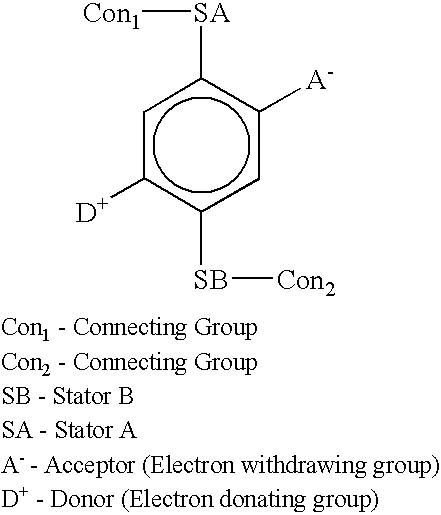
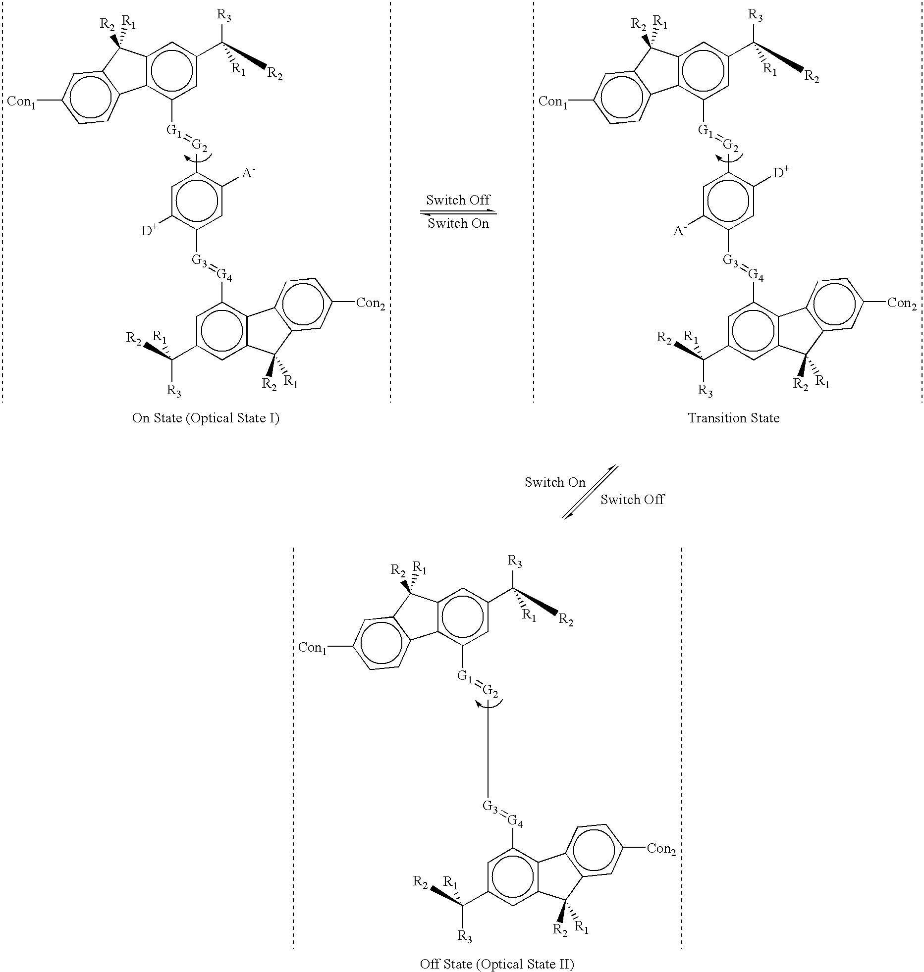
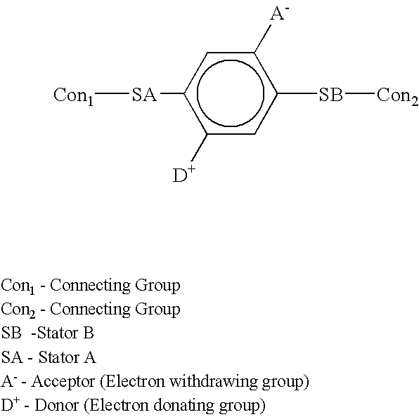
show two different orientations for switching the molecules. Example 1a below depicts a first generic molecular example for this Model 1. ##STR1##


PUM

PropertyMeasurementUnit
sizeaaaaaaaaaa
heightsaaaaaaaaaa
angleaaaaaaaaaa

Abstract

Molecular systems are provided for electric field activated switches, such as optical switches. The molecular system has an electric field induced band gap change that occurs via one of the following mechanisms: (1) molecular conformation change; (2) change of extended conjugation via chemical bonding change to change the band gap; or (3) molecular folding or stretching. Nanometer-scale reversible optical switches are thus provided that can be assembled easily to make a variety of optical devices, including optical displays.

Description

The present application is an improvement over the foregoing applications in that it is directed to classes of molecules that provide switching from one state to a different state, characterized by a change in the optical properties, including color, of the molecules. In the case of color switching, the present invention turns ink or dye or pigment molecules into active opto-electronic devices that can be switched by an external electric field.The present invention relates generally to optical devices whose functional length scales are measured in nanometers, and, more particularly, to classes of molecules that provide optical switching. Optical devices both of micrometer and nanometer scale may be constructed in accordance with the teachings herein.The area of molecular electronics is in its infancy. To date, there have been two convincing demonstrations of molecules as electronic switches published in the technical literature; see, C. P. Collier et al., Science, Vol. 285, pp. 391-...

Claims


Application Information

Patent Timeline
Patent Type & Authority Patents(United States)
IPC IPC(8): G02F1/01G02F1/15G02F1/17G11C13/02G02B26/02G11C23/00
CPCB82Y10/00G02B26/026G02F1/15G02F1/174G11C13/0014G11C13/02G11C23/00G11C13/04G11C2213/14G11C2213/77G11C2213/81G02F1/061
Inventor ZHANG, XIAO-ANWILLIAMS, R. STANLEYVINCENT, KENT D.
Owner HEWLETT PACKARD DEV CO LP
Why Eureka
Try Eureka