Magnetron plasma processing apparatus

a plasma processing and plasma technology, applied in the field of magnetic plasma processing apparatus, can solve the problems of insufficient plasma uniformity, charge-up damage, etc., and achieve the effect of increasing the plasma density of the processing spa

Inactive Publication Date: 2004-07-20
TOKYO ELECTRON LTD +1
View PDF4 Cites 33 Cited by
  • Summary
  • Abstract
  • Description
  • Claims
  • Application Information

AI Technical Summary

Benefits of technology

It is an object of the present invention to provide a magnetron plasma processing apparatus which can form a locally strong magnetic fiel

Problems solved by technology

As a uniform horizontal magnetic field is not always formed in the above apparatus, plasma uniformity is not sufficient.
Thus, a nonuniform etching rate, charge-up damage, and the like may occur.
In practice, however, this cannot make the plasma density sufficiently uniform over a wide range.
When, however, an insulating film such as an oxide film is to be etched, to avoid charge-up damage, the magne

Method used


Image

  • Magnetron plasma processing apparatus
  • Magnetron plasma processing apparatus
  • Magnetron plasma processing apparatus

Examples


Embodiment Construction

The embodiments of the present invention will be described with reference to the accompanying drawings.

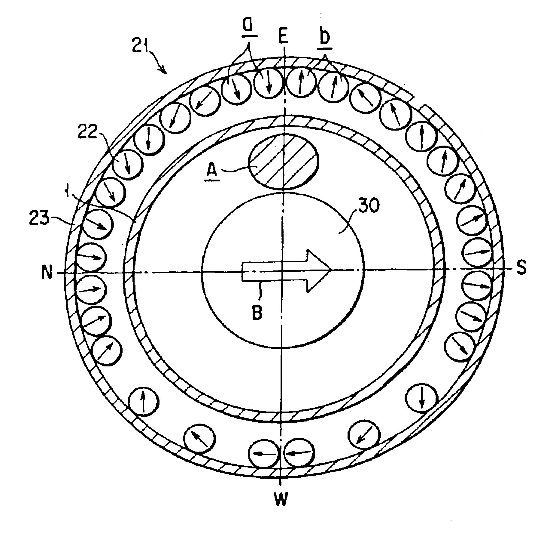
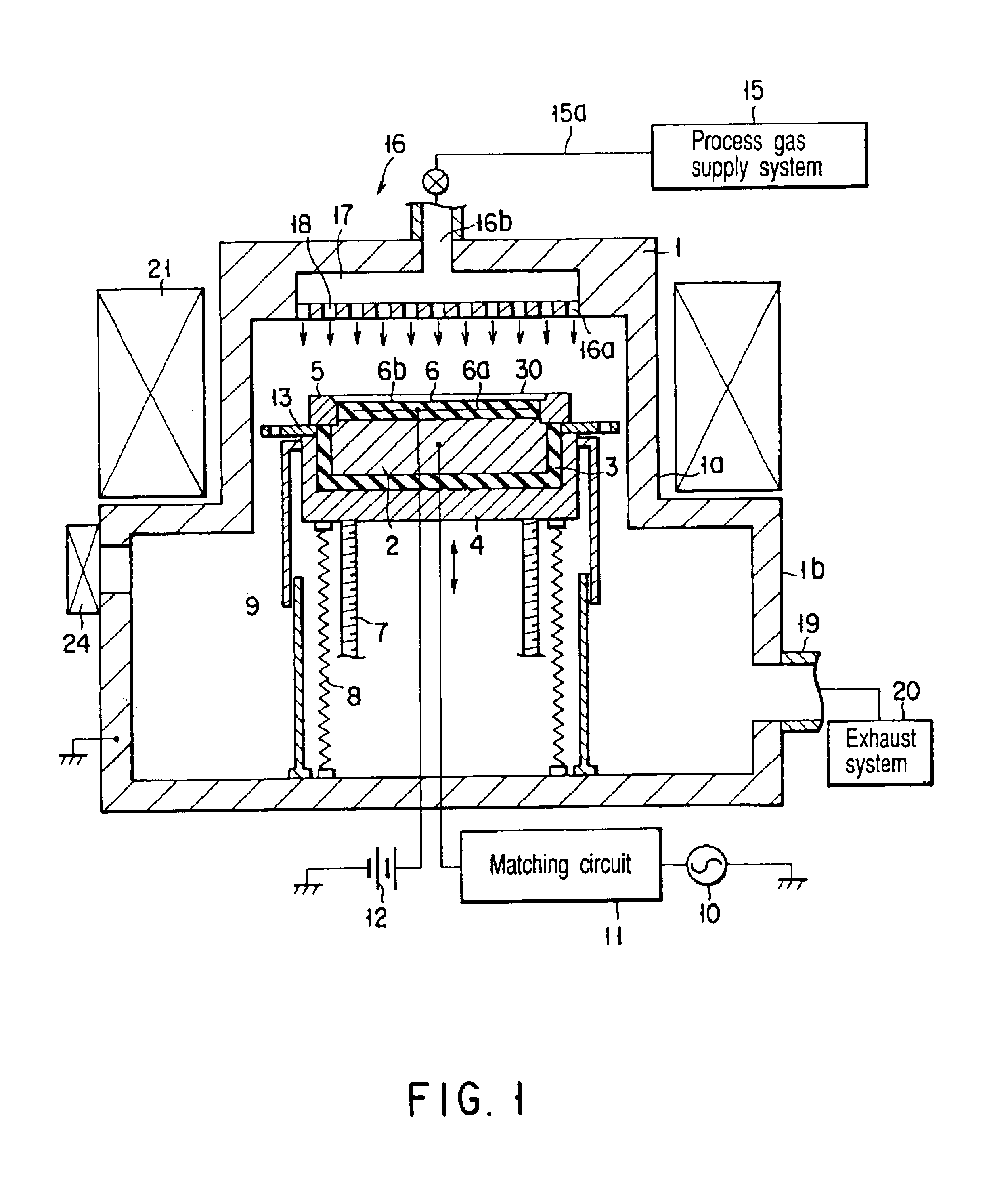
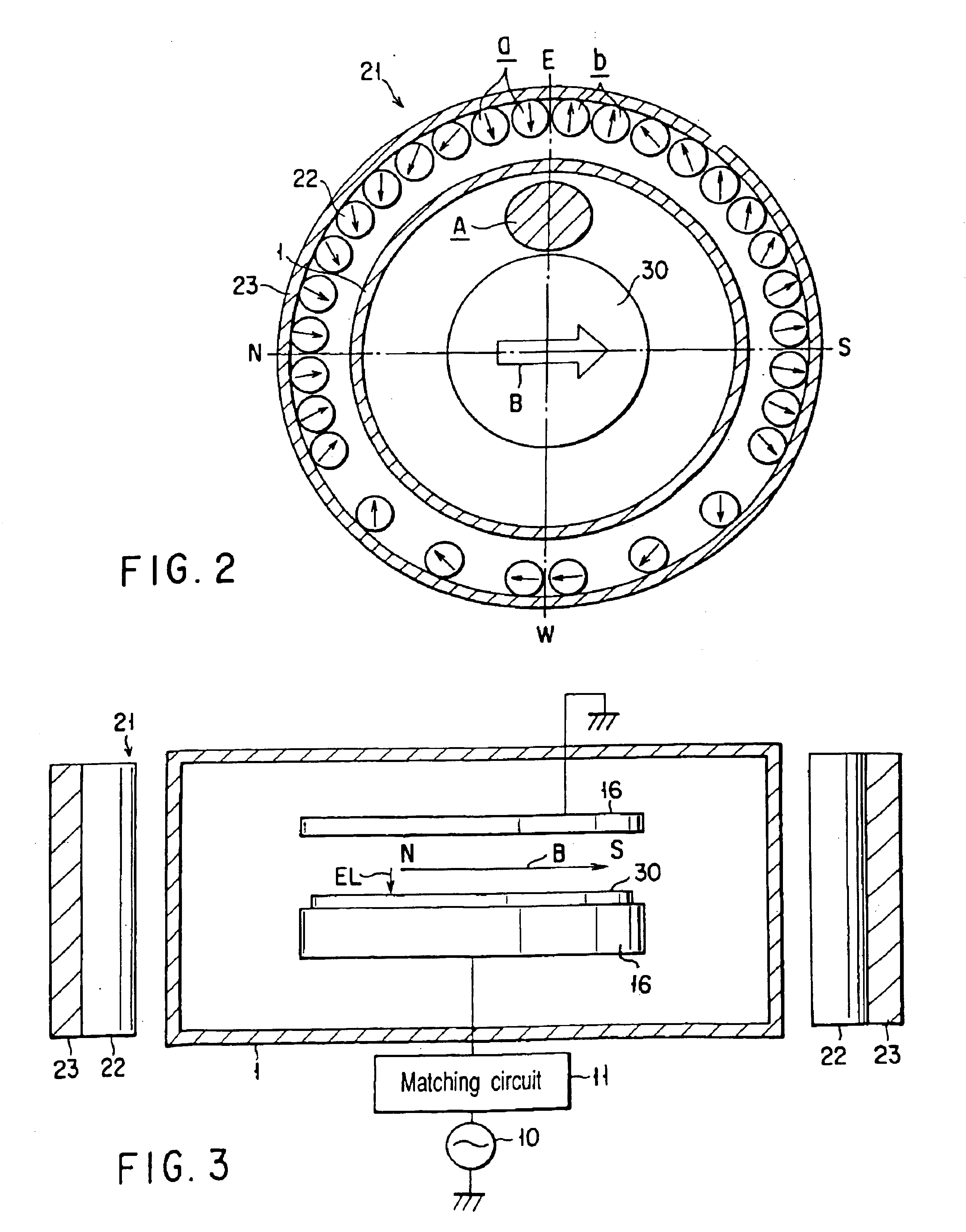
FIG. 1 is a sectional view showing a magnetron plasma etching apparatus according to an embodiment of the present invention. This etching apparatus has an airtight chamber 1. The chamber 1 forms a stepped cylindrical shape constituted by a small-diameter upper portion 1a and large-diameter lower portion 1b. The wall of the chamber 1 is made of a conductor such as aluminum. A support table 2 for horizontally supporting a semiconductor wafer 30 as a target object thereon is arranged in the chamber 1. For example, the support table 2 is formed of an aluminum circular plate, and is supported on a conductive support base 4 through an insulating plate 3. A conductive focus ring 5 made of, e.g., single-crystal silicon, is arranged on the periphery of an upper surface of the support table 2. The support table 2 and support base 4 can be vertically moved with respect to the chamber 1 by a k...


PUM

PropertyMeasurementUnit
Lengthaaaaaaaaaa
Lengthaaaaaaaaaa
Pressureaaaaaaaaaa

Abstract

When a substrate 30 is to be subjected to a magnetron plasma process, a dipole ring magnet 21 is provided, in which a large number of anisotropic segment magnets 22 are arranged in a ring-like shape around the outer wall of a chamber 1. A magnetic field gradient, wherein the magnetic field strength decreases from the E pole side toward the W pole side in a direction perpendicular to a magnetic field direction B, is formed in a plane perpendicular to the direction of an electric field between a pair of electrodes separated from each other. The anisotropic segment magnets have a first section a including anisotropic segment magnets arranged in the vicinity of a region A located outside an E pole side end of the process substrate with an N pole thereof being directed toward this region, and a second portion b including anisotropic segment magnets arranged with an S pole thereof being directed toward this region, to locally increase the magnetic field strengths of the first and second regions.

Description

The present invention relates to a magnetron plasma processing apparatus for processing a target substrate such as a semiconductor wafer with a magnetron plasma.In recent years, a magnetron plasma etching apparatus for performing micropattern etching by generating a high-density plasma in a comparatively low-pressure atmosphere has been put into practical use. In this apparatus, a permanent magnet is arranged above a chamber. The magnetic field produced by the permanent magnet is applied horizontally to a semiconductor wafer. An RF electric field perpendicular to the magnetic field is simultaneously applied to the semiconductor wafer. The drift motion of electrons caused upon application of the magnetic and electric fields is utilized to etch the semiconductor wafer with a very high efficiency.In the magnetron plasma, what contributes to the drift motion of electrons is a magnetic field perpendicular to the electric field, i.e., a magnetic field horizontal to the semiconductor wafer...

Claims


Application Information

Patent Timeline
IPC IPC(8): H01J37/34H01J37/32H01L21/302C23F4/00H01L21/3065H05H1/46
CPCH01J37/3266H01J37/3408H01L21/3065
Inventor YAMASAKI, TOMOMIKIMURA, HIDETOSHIARAMI, JUNICHIONO, HIROOKOSHIISHI, AKIRAMIYATA, KOJI
Owner TOKYO ELECTRON LTD
Why Eureka
Try Eureka