Hall sensor array for measuring a magnetic field with offset compensation

a sensor array and offset compensation technology, applied in the field of hall sensors, can solve the problems of inhomogeneity or faults in the active region of semiconductor materials, inability to completely avoid inhomogeneities, and the scattering of traditional hall sensor elements, and achieve the effect of less complicated manufacturing

Inactive Publication Date: 2004-07-27
FRAUNHOFER GESELLSCHAFT ZUR FOERDERUNG DER ANGEWANDTEN FORSCHUNG EV
View PDF11 Cites 153 Cited by
  • Summary
  • Abstract
  • Description
  • Claims
  • Application Information

AI Technical Summary

Benefits of technology

to provide an improved Hall sensor array...

Problems solved by technology

As is known, inhomogeneities or faults in the semiconductor material of the active region often arise in the manufacturing processes of semiconductor structures due to the nature of production.
Even with very refined manufacturing methods, these inhomogeneities cannot be avoided completely.
These inhomogeneities are often the cause of an offset of the sensor signal.
Owing to the strong dependence of the offset signal on the inhomogeneities, traditional Hall sensor elements are subject to considerable scatter from one element to another.
In addition there is a marked adverse effect or the sensitivity and measurement accuracy...

Method used


Image

  • Hall sensor array for measuring a magnetic field with offset compensation
  • Hall sensor array for measuring a magnetic field with offset compensation
  • Hall sensor array for measuring a magnetic field with offset compensation

Examples


Embodiment Construction

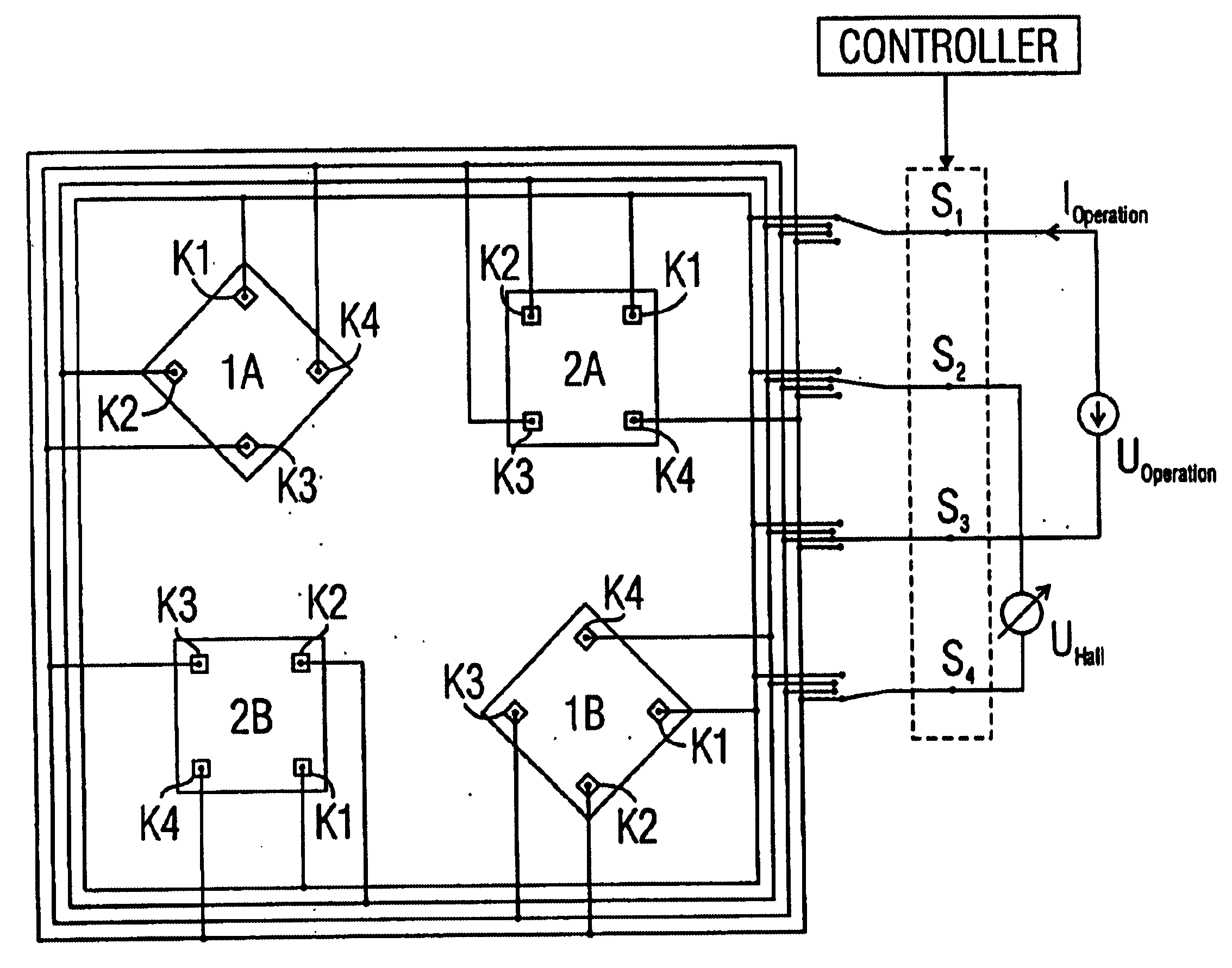
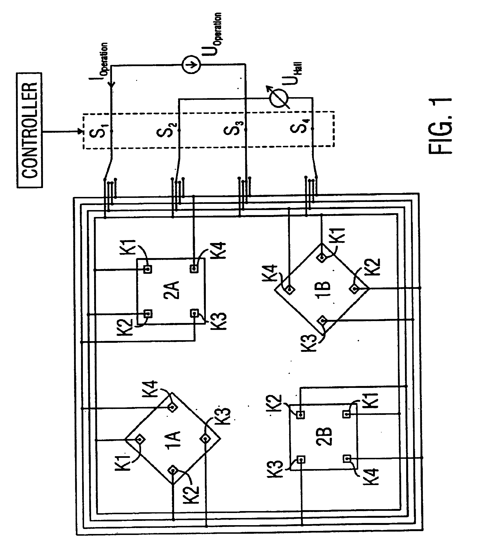
The general structure of a Hall sensor array with two pairs of Hall sensor elements will now be described making reference to FIG. 1.

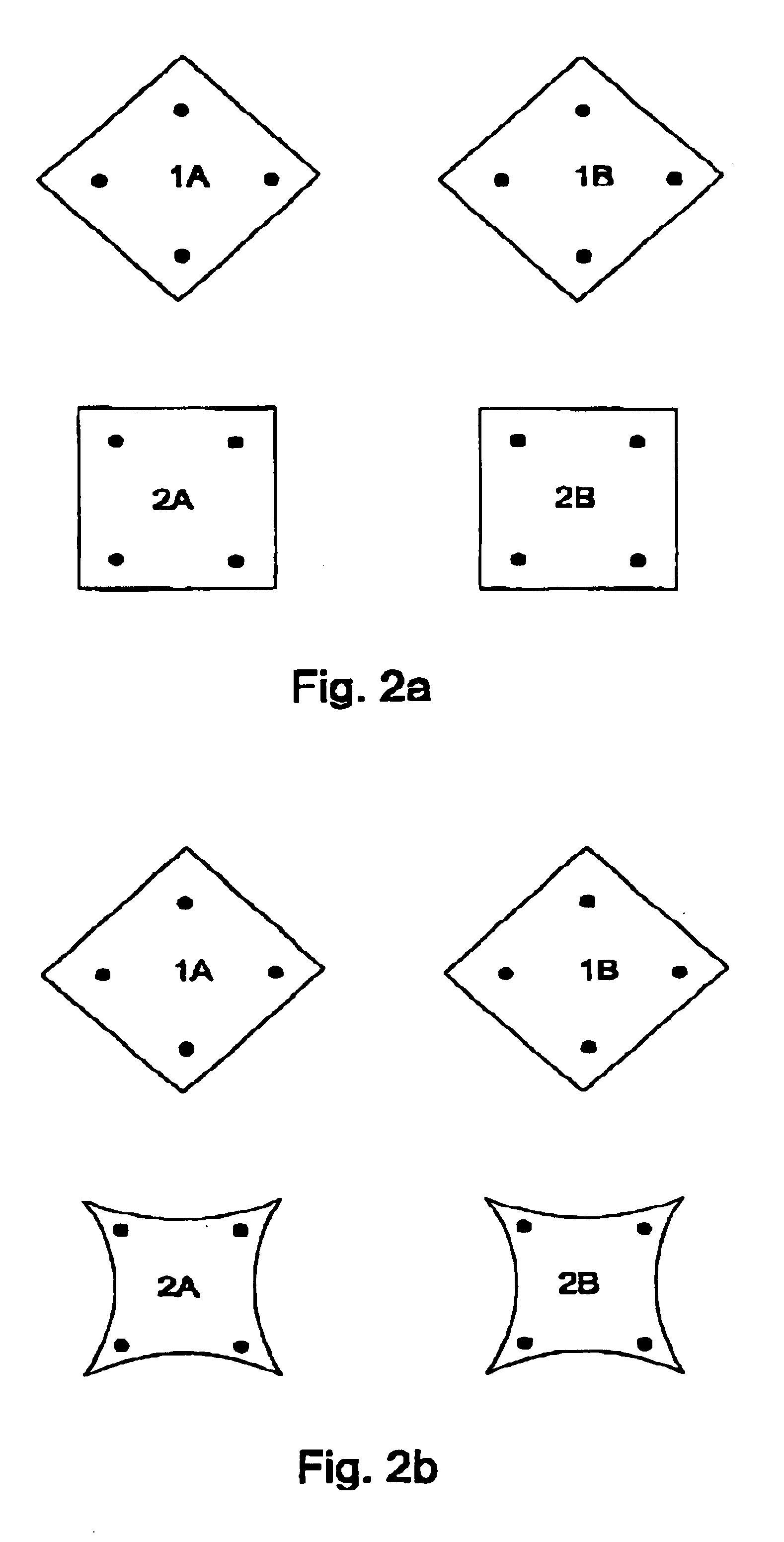
On a semiconductor substrate, which is preferably p-doped, four rectangular active semiconductor regions are introduced, these usually being n-doped. Contact electrodes K1, K2, K3, K4, which are generally obtained by n.sup.+ -doping, are preferably arranged in the corners of the n-doped active region. The contact electrodes K1, K2, K3, K4 in the n-doped active region are arranged diagonally opposite each other in pairs, two contact electrodes K1, K3 serving to feed in the operating current and the other two contact electrodes K2, K4 to tap off the Hall voltage. The active regions constitute the individual Hall sensor elements 1A, 2A, 1B, 2B. In the Hall sensor array with four Hall sensor elements shown in FIG. 1 the Hall sensor elements 1A, 1B and the Hall sensor elements 2A, 2B respectively constitute a Hall sensor element pair.

FIG. 1 shows an embodim...


PUM


Abstract

A Hall sensor array for offset-compensated magnetic field measurement comprises a first and at least one additional pair of Hall sensor elements. Each Hall sensor element has four terminals, of which two act as power supply terminals for supplying an operating current and two act as measurement terminals for measuring a Hall voltage. Respective first supply terminals of each Hall sensor element are connected together and to a first terminal of a common voltage source and respective second supply terminals of each Hall sensor element are connected together and to a second terminal of the common voltage source so that the common voltage source supplies an operating current for the Hall sensor elements. The Hall sensor elements are operated in the spinning current mode so that the offset voltages of the Hall sensor elements approximately cancel one another out in a revolution so that the Hall signal contributions which actually depend on the magnetic field remain.

Description

1. Field of the InventionThe present invention relates generally to Hall sensors and in particular to the arrangement and control of several Hall sensor elements in a Hall sensor array for magnetic field measurement with offset compensation.2. Description of Prior ArtAn individual Hall sensor element generally consists of an n-doped active semiconductor region on a p-doped semiconductor substrate. The n-doped active region is normally connected to an external control logic via four contact electrodes or contact terminals which are arranged diagonally opposite one another in the active region. The four contact electrodes of the Hall sensor element subdivide into two facing control current contact electrodes, which serve to generate a current flow through the active region, and two facing voltage tapping contact electrodes, which serve to tap a Hall voltage, which arises when a magnetic field is applied at right angles to the current flow in the active region, to act as a sensor signa...

Claims


Application Information

Patent Timeline
IPC IPC(8): G01R33/06G01R33/07H01L27/22H01L43/06
CPCG01R33/0094G01R33/07G01R33/075
Inventor HOHE, HANS-PETERWEBER, NORBERTSAUERER, JOSEF
Owner FRAUNHOFER GESELLSCHAFT ZUR FOERDERUNG DER ANGEWANDTEN FORSCHUNG EV
Why Eureka
Try Eureka