ONO fabrication process for reducing oxygen vacancy content in bottom oxide layer in flash memory devices

a technology of flash memory and oxide layer, which is applied in the direction of semiconductor devices, basic electric elements, electrical equipment, etc., can solve the problem of limiting the scaling down of the total physical thickness of the ono layer, and achieve the reduction of the number of e' centers and dangling bonds, and the oxygen content is high.

Inactive Publication Date: 2004-10-12
LONGITUDE FLASH MEMORY SOLUTIONS LTD
View PDF10 Cites 50 Cited by
  • Summary
  • Abstract
  • Description
  • Claims
  • Application Information

AI Technical Summary

Benefits of technology

Thus, according to the present invention, by providing an increased oxygen content in the bottom oxide layer of the ONO structure in a flash memory device, a bottom oxide layer may be fabricated without creation of interface states resulting from oxygen vacancies, E' centers and dangling bonds, which could provide charge leakage paths from the charge-storage layer. The present invention can be carried out in a cluster tool. The present invention provides advantages such as (1) formation of a bottom oxide layer with a higher oxygen content and a reduced oxygen vacancy content, reduced numbers of E' centers and dangling bonds; (2) allowing selection of any of a number of different methods for obtainin

Problems solved by technology

However, as the ONO layer is made physically thinner, leakage currents through the ONO layer may increase, which limits the scaling down of the total physical thickness of the ONO layer.
While the recent advances

Method used


Image

  • ONO fabrication process for reducing oxygen vacancy content in bottom oxide layer in flash memory devices
  • ONO fabrication process for reducing oxygen vacancy content in bottom oxide layer in flash memory devices
  • ONO fabrication process for reducing oxygen vacancy content in bottom oxide layer in flash memory devices

Examples


first embodiment

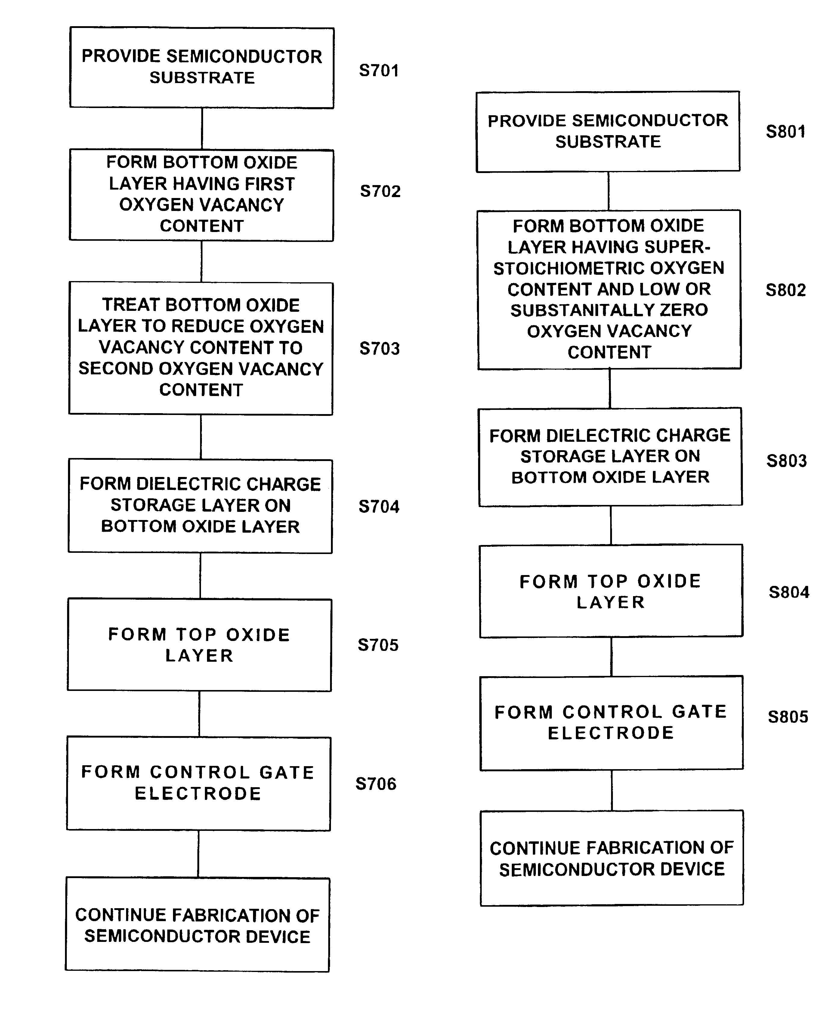
The present invention broadly includes two embodiments. In the present invention, shown schematically in FIG. 7, a bottom oxide layer 28 is formed by a conventional process to include a first oxygen vacancy content, and is thereafter treated to reduce the oxygen vacancy content from the first oxygen vacancy content to a second oxygen vacancy content. In this embodiment, the bottom oxide layer having the second, reduced oxygen vacancy content exhibits a reduced charge leakage relative to the bottom oxide layer having the first, higher oxygen vacancy content. In one embodiment, the bottom oxide layer having the second, reduced oxygen content has a super-stoichiometric oxygen content.

second embodiment

In the present invention, shown schematically in FIG. 8, a bottom oxide layer 28 is formed by processes which include strongly oxidizing conditions, which provide the bottom oxide layer 28 with a super-stoichiometric oxygen content and thereby an oxygen vacancy content which is reduced relative to that of a bottom oxide layer made by a conventional process. In one embodiment, the bottom oxide layer 28 is formed having a substantially zero oxygen vacancy content. In one embodiment, the super-stoichiometric oxygen content provides an increased oxygen content relative to the oxygen content in a conventional bottom oxide. In one embodiment, the bottom oxide layer having the super-stoichiometric oxygen content exhibits a reduced charge leakage relative to a conventional bottom oxide layer.

The first step of both embodiments is the same. In the first step of the present invention, shown schematically in FIG. 7 as step 701 and in FIG. 8 as step 801, a semiconductor substrate is provided. Th...


PUM


Abstract

Process for fabricating a SONOS flash memory device, including in one embodiment, forming a bottom oxide layer of an ONO structure on a semiconductor substrate, wherein the bottom oxide layer has a first oxygen vacancy content; treating the bottom oxide layer to decrease the first oxygen vacancy content to a second oxygen vacancy content; and depositing a dielectric charge-storage layer on the bottom oxide layer. In another embodiment, a process for fabricating a SONOS flash memory device includes forming a bottom oxide layer of an ONO structure on the semiconductor substrate under strongly oxidizing conditions, wherein the bottom oxide layer has a super-stoichiometric oxygen content and an oxygen vacancy content reduced relative to a bottom oxide layer formed by a conventional process; and depositing a dielectric charge-storage layer on the bottom oxide layer.

Description

The present invention relates to a process for preparation of a SONOS flash memory device including an ONO structure in which the bottom oxide layer exhibits reduced charge leakage. The bottom oxide layer is provided with increased oxygen content and / or reduced oxygen vacancy content.Non-volatile memory devices are currently in widespread use in electronic components that require the retention of information when electrical power is terminated. Non-volatile memory devices include read-only-memory (ROM), programmable-read-only memory (PROM), erasable-programmable-read-only memory (EPROM), and electrically-erasable-programmable-read-only-memory (EEPROM) devices. EEPROM devices differ from other non-volatile memory devices in that they can be electrically programmed and erased. Flash EEPROM devices are similar to EEPROM devices in that memory cells can be programmed and erased electrically. However, flash EEPROM devices enable the erasing of all memory cells in the device using a singl...

Claims


Application Information

Patent Timeline
IPC IPC(8): H01L21/02H01L21/28H01L21/336H01L21/314
CPCH01L21/28282H01L29/66833H01L21/3144H01L29/40117H01L21/02183H01L21/02271H01L21/02312H01L21/0217H01L21/02255H01L21/02238H01L21/02252H01L21/022H01L21/02274H01L21/02301H01L21/02178H01L21/02337
Inventor PARK, JAEYONGSHIRAIWA, HIDEHIKOHALLIYAL, ARVINDYANG, JEAN Y.KANG, INKUKKAMAL, TAZRIENJAFARPOUR, AMIR H.
Owner LONGITUDE FLASH MEMORY SOLUTIONS LTD
Why Eureka
Try Eureka