
Methods and compositions for optimizing interfacial properties of magnetoresistive sensors

a technology of magnetoresistive sensors and compositions, applied in magnetic recording, fluid speed measurement, record information storage, etc., can solve problems such as inability to explain, and achieve the effects of minimizing the difference in electronegativities between layers and spacers, extending the useful lifetime of spin valve and gmr sensors, and minimizing electromigration

Inactive Publication Date: 2004-12-07
WESTERN DIGITAL TECH INC
View PDF3 Cites 173 Cited by
  • Summary
  • Abstract
  • Description
  • Claims
  • Application Information

AI Technical Summary

Benefits of technology

is to provide conductive spacers which minimize electromigration in the FM and spacer layers, which extend the useful lifetimes of spin valve and GMR sensors.
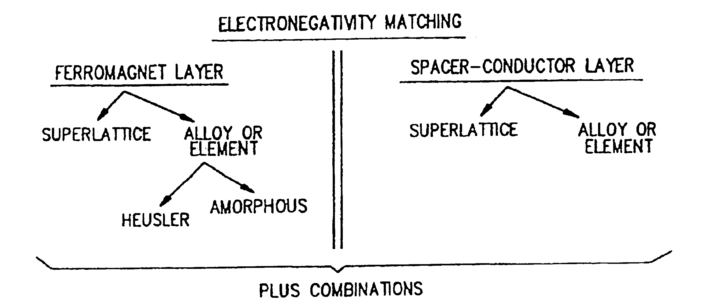
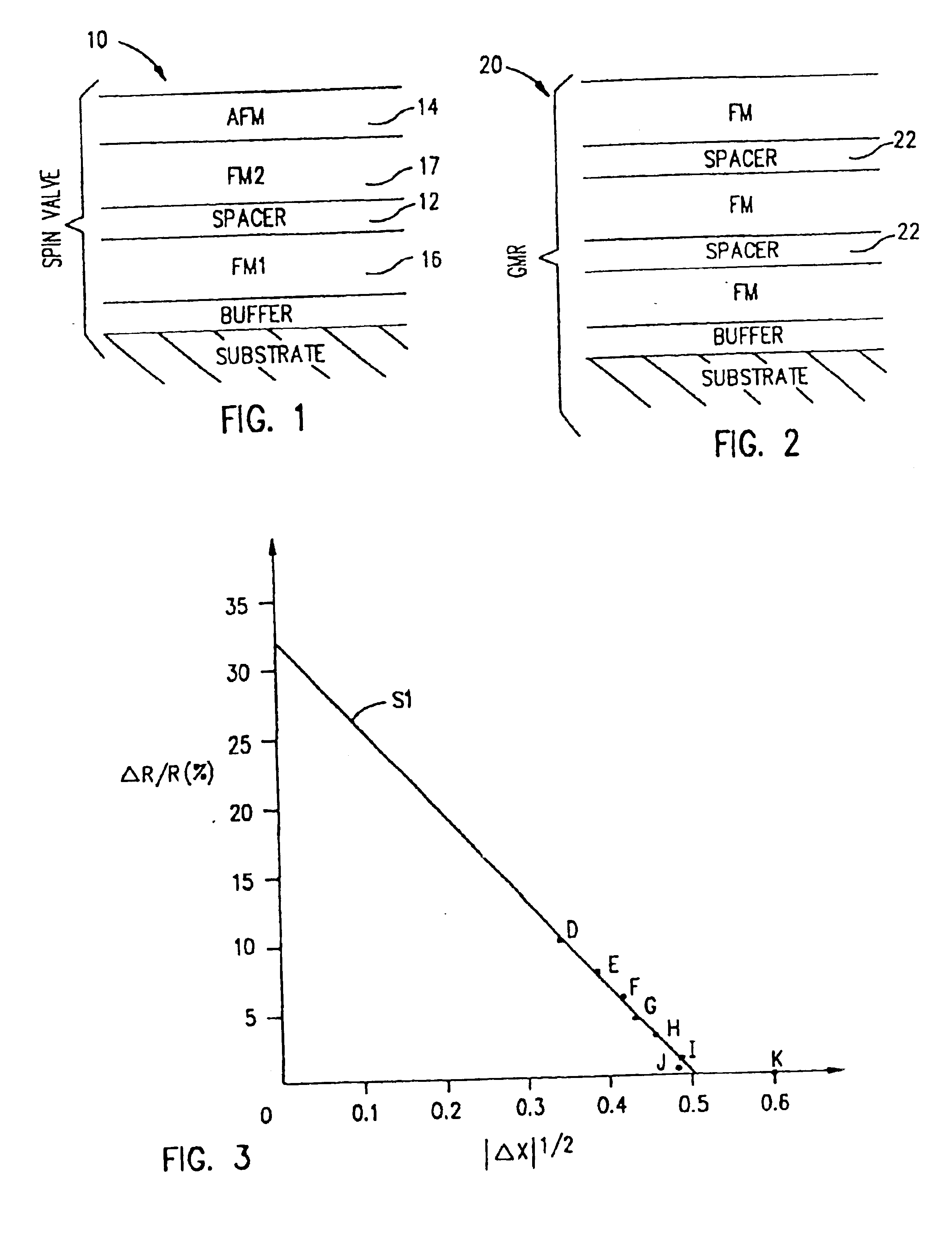
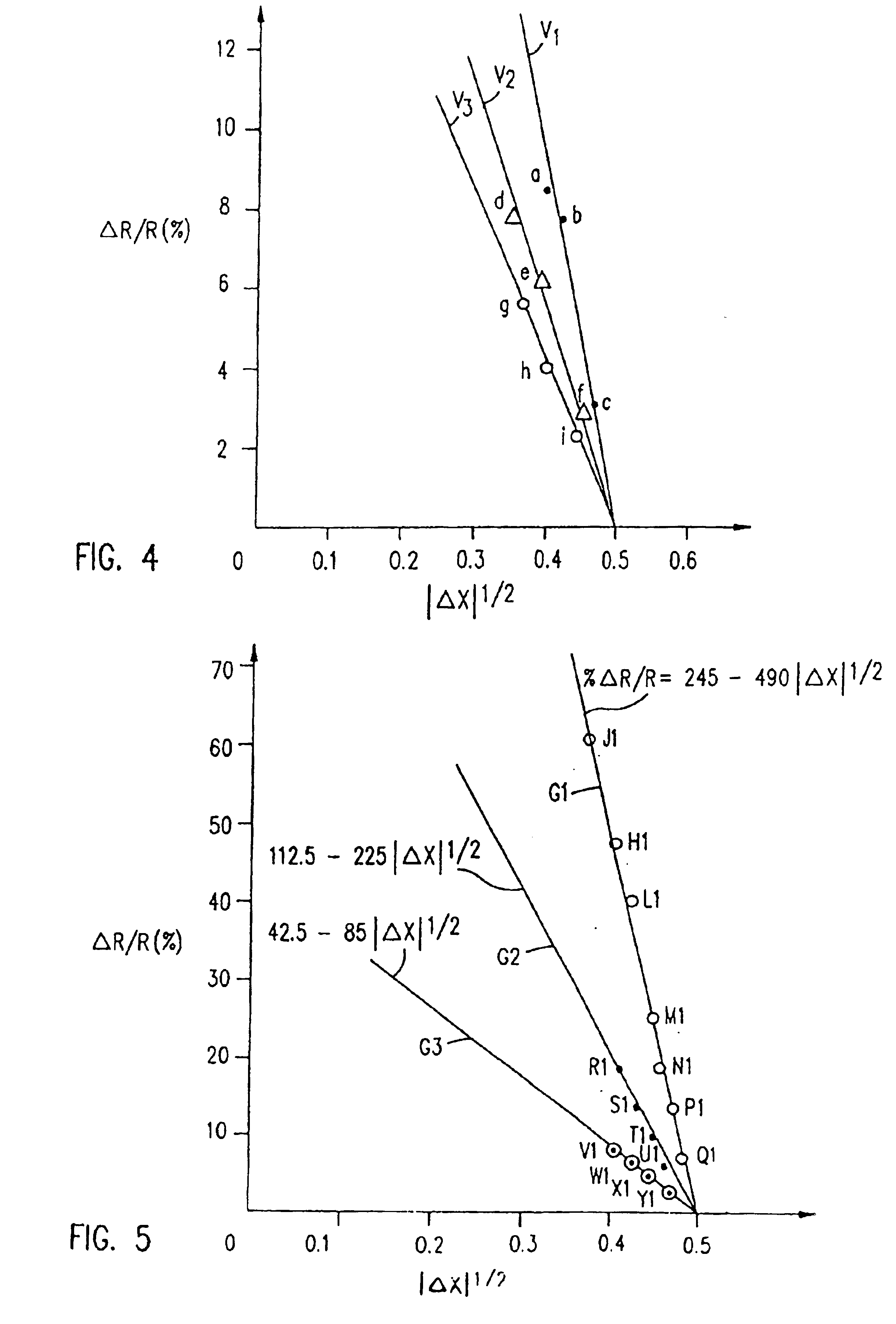
Another object is to provide for multiple interfacial matching of an FM layer with its contacting conductive spacers. In accordance with this invention, spin valve sensors and GMR sensors are made with layers of FM material and conductive spacers interposed between the FM layers. The difference in electronegativities between the layers and spacers is minimized. A relatively low resistivity and / or a large mean free path is provided by the conductive spacer material. As a result of these conditions, the .DELTA.R / R of the sensor is maximized. The novel sensor is also corrosion resistant, exhibits greater chemical and thermal stability, and signal output of the sensor device is increased.
A method for optimizing the interfacial properties of a magnetoresistive sensor, such as a GMR or spin valve, is disclosed. The method includes selecting one or more FM layers having at least a first electronegativity, and selecting one or more conductive spacers having at least a second electronegativity, such that the selecting steps include the step of substantially matching or minimizing the difference between the first and second electronegativities and thereby minimizing the difference between the electronegativities of the selected spacers and FM layers.

Problems solved by technology

However, there does not currently exist an explanation of the main factors controlling the magnitude of the sensor response, as characterized by .DELTA.R / R, as it relates to the required properties of the conductive spacers and ferromagnetic (FM) layers constituting such device.

Method used


Image

  • Methods and compositions for optimizing interfacial properties of magnetoresistive sensors
  • Methods and compositions for optimizing interfacial properties of magnetoresistive sensors
  • Methods and compositions for optimizing interfacial properties of magnetoresistive sensors

Examples


example 2

Another aspect of the invention concerns the use of materials exhibiting superlattice structures for FM layers and spacers in GMR and spin valve sensors. The prior art does not teach or disclose the use of such superlattice structures in MR sensors. Significant advantages in MR device performance can be achieved with such superlattice structures, even without the matching of .chi. values. For example, Ni.sub.3 Mn, a ferromagnetic superlattice intermetallic compound having an electronegativity of 2.01, may be matched with Cu.sub.3 Pt, as described in Example 1. The matching of two superlattice structures is desirable in that these ordered structures will improve the thermal stability of sensors containing them. It is believed that this is due to the additional external thermal energy that would be required to disorder one or both superlattice structures before the elements contained in the superlattice would be free to diffuse at the interface. This additional energy ranges between 0...

example 3

A subsequent inquiry may then be made as to whether there exists another ferromagnet with other desirable characteristics, such as minimal magnetostriction (.lambda..sub.s), higher corrosion resistance, and / or lower resistivity than Ni.sub.3 Mn. Ni.sub.3 Fe, also a superlattice alloy, with an electronegativity of 2.07, may in certain applications present a more desirable match than Ni.sub.3 Mn, due to low coercivity (H.sub.c), low .lambda..sub.s and superior corrosion resistance and may be matched with a CuAu superlattice having an .chi. of 2.07.

example 4

This example identifies conductive spacer alloys useful for the matching or minimizing the .DELTA..chi. values between the spacer alloys and appropriate ferromagnetic elements or alloys thereof.

In addition to CuAu and CuPt alloys and their superlattice compositions referred to previously, binary, ternary or higher Ig order alloys of elements such as Cu, Ag, Au, Pt, Pd, Ir, Rh and Ru may be used to match appropriate FMs and provide .chi. values ranging from approximately 1.89 to 2.33. Such alloys may be used to fabricate various devices, including but not limited to spin valve and GMR sensors, based on the electronegativity matching or minimizing of the differences in electronegativities of the present invention. Other superlattice alloys similar to CuPt and CuAu that exhibit ordering phenomena, such as Ag.sub.3 Pt and AgPt, may also be used for implementing this invention.


PUM


Abstract

A method for maximizing the interfacial properties of magnetoresistive sensors, such as spin valve and GMR sensors used in storage devices, comprises selecting the materials for ferromagnetic layers and for electrically conductive spacers that are interposed between the ferromagnetic layers. The electronegativities of the selected materials are substantially matched so that an absolute value of the differences in electronegativities is minimized. The conductive spacer material provides a relatively low resistivity and a large mean free path. The sensors experience greater chemical and thermal stability, are corrosion resistant, and realize an increased signal output.

Description

This invention relates to methods and compositions for optimizing the interfacial properties of magnetoresistive sensors, and specifically data storage devices such as spin valve sensors and giant magnetoresistive (GMR) sensors.DESCRIPTION OF THE PRIOR ARTSignificant progress has occurred over the past two decades in the design of multilayered nanostructured thin film systems. Large GMR current-in-plane (CIP) effects have been described in a Fe / Cr multilayered system, approximating a magnetoresistance effect (.DELTA.R / R) of 100 percent, which is a change by a factor of two in resistance with an adequate external field. Since then, many other multilayer GMR and spin valve sensors have been explored. To date, the highest GMR effect is in the Fe / Cr system and is approximately 150 percent at a measurement temperature of 5.degree. K, and remains the largest value observed at any temperature to date. Both the GMR and spin valve effects are characterized by .DELTA.R / R, which is defined as ...

Claims


Application Information

Patent Timeline
IPC IPC(8): G01R33/06G01R33/09H01F41/30H01F41/14G11B5/39H01L43/00H01L43/10G11B5/40B81B1/00B81C99/00
CPCB82Y10/00B82Y25/00B82Y40/00G01R33/093H01L43/10H01F41/302G11B5/3903G11B5/40G11B2005/3996H10N50/85H10N50/10
Inventor NEPELA, DANIEL A.
Owner WESTERN DIGITAL TECH INC
Learn More