Method and apparatus for modeling a neural synapse function by utilizing a single conventional MOSFET

a neural synapse and model technology, applied in the field of methods and apparatus, can solve the problems affecting the accuracy of the model, and requiring much higher electric fields and supply voltages than normal, so as to achieve the effect of limiting the applicability of the model

Inactive Publication Date: 2004-12-07
TEXAS INSTR INC
View PDF28 Cites 45 Cited by
  • Summary
  • Abstract
  • Description
  • Claims
  • Application Information

AI Technical Summary

Benefits of technology

Consequently, by the merit of relationship in Eq. (1.5), a single MOSFET device offers good potential and yields a rather simple method for modeling a synapse function in hardware.
Finally, the current output means (36) construct a current mirror between the neuron load (100) and (101) to provide output current proportional to the sum of all synaptic output currents summed at node (99) without affecting said synaptic currents (as i.sub.D41 or overall synaptic current i.sub.D100). The latter also provide a current sink source (102 and 103) compatible with the design of the current input(s) (like 33) of the described synapse(s) to allow for easy interconnection. It should be noted that, although, means (36) do not implement any specific hard-limiting function, as shown in this embodiment, it is inherent property of the circuit implemented by (101),(102) and (103) that it will, in fact, limit the overall circuit output due to two main factors:

Problems solved by technology

In implementing real-time digital signal processing applications, the conventional VLSI technology has many limitations with regard to chip area and its speed, due to complexity of both hardware and software processing algorithms.
For example, at the voltages and oxide thicknesses used in conventional silicon MOS processing, the tunneling probability is exceedingly small, likewise hot-electron-injection requires much higher electric fields and supply voltages than normal.
The latter is in direct conflict with the tendency of lowering supply voltages with the constant decrease of the device geometries and increase of the scale of integration.
Therefore, in general practice, those solutions do not allow for easy on-chip integration with other integrated circuit applications implemented on most widely used conventional CMOS processes.

Method used


Image

  • Method and apparatus for modeling a neural synapse function by utilizing a single conventional MOSFET
  • Method and apparatus for modeling a neural synapse function by utilizing a single conventional MOSFET
  • Method and apparatus for modeling a neural synapse function by utilizing a single conventional MOSFET

Examples


Embodiment Construction

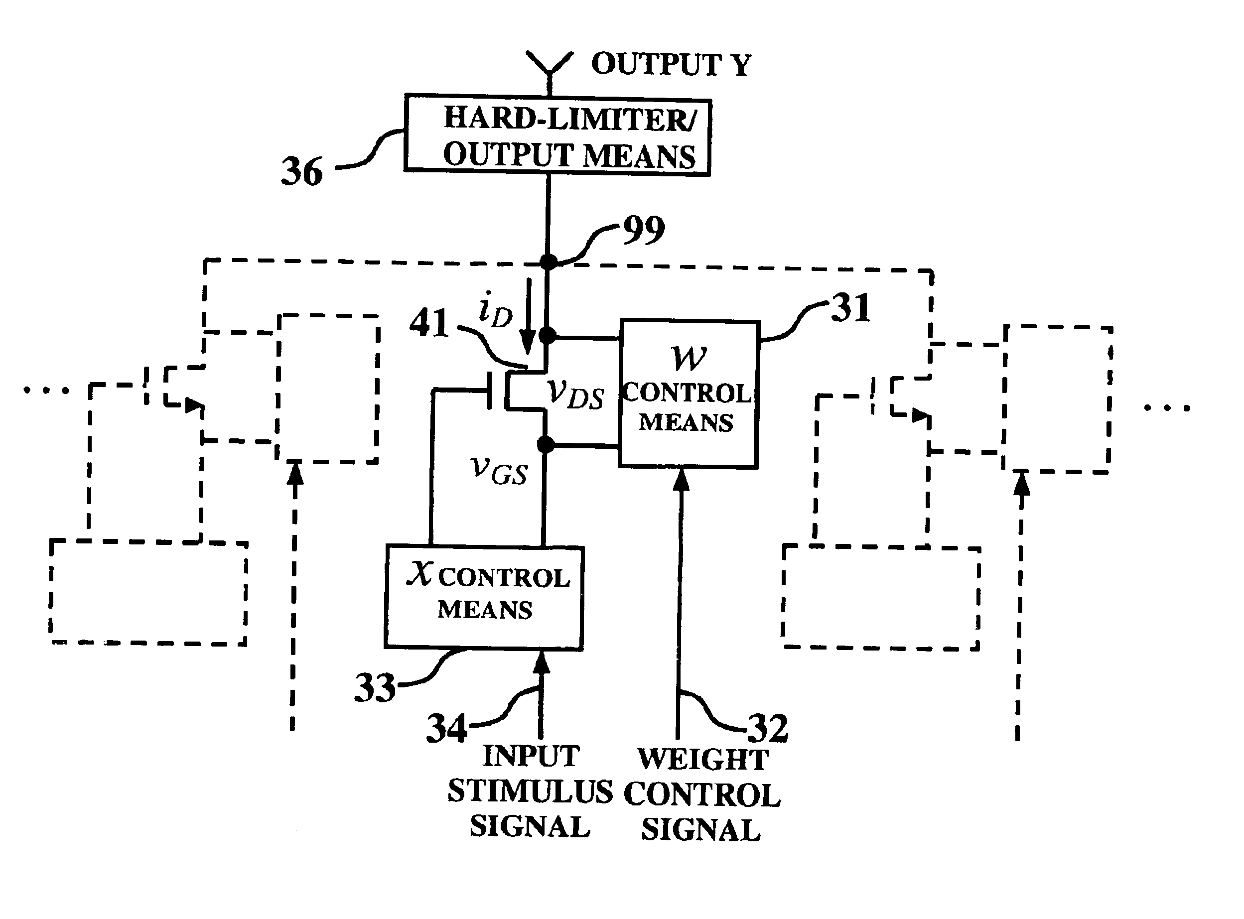
The essence of the invention herein will be obvious to those of ordinary skill in the art after examining related computational equations on which the invention is based. Further below, the preferred embodiment of the present invention will be explained with reference to the accompanying drawings.

I. Method

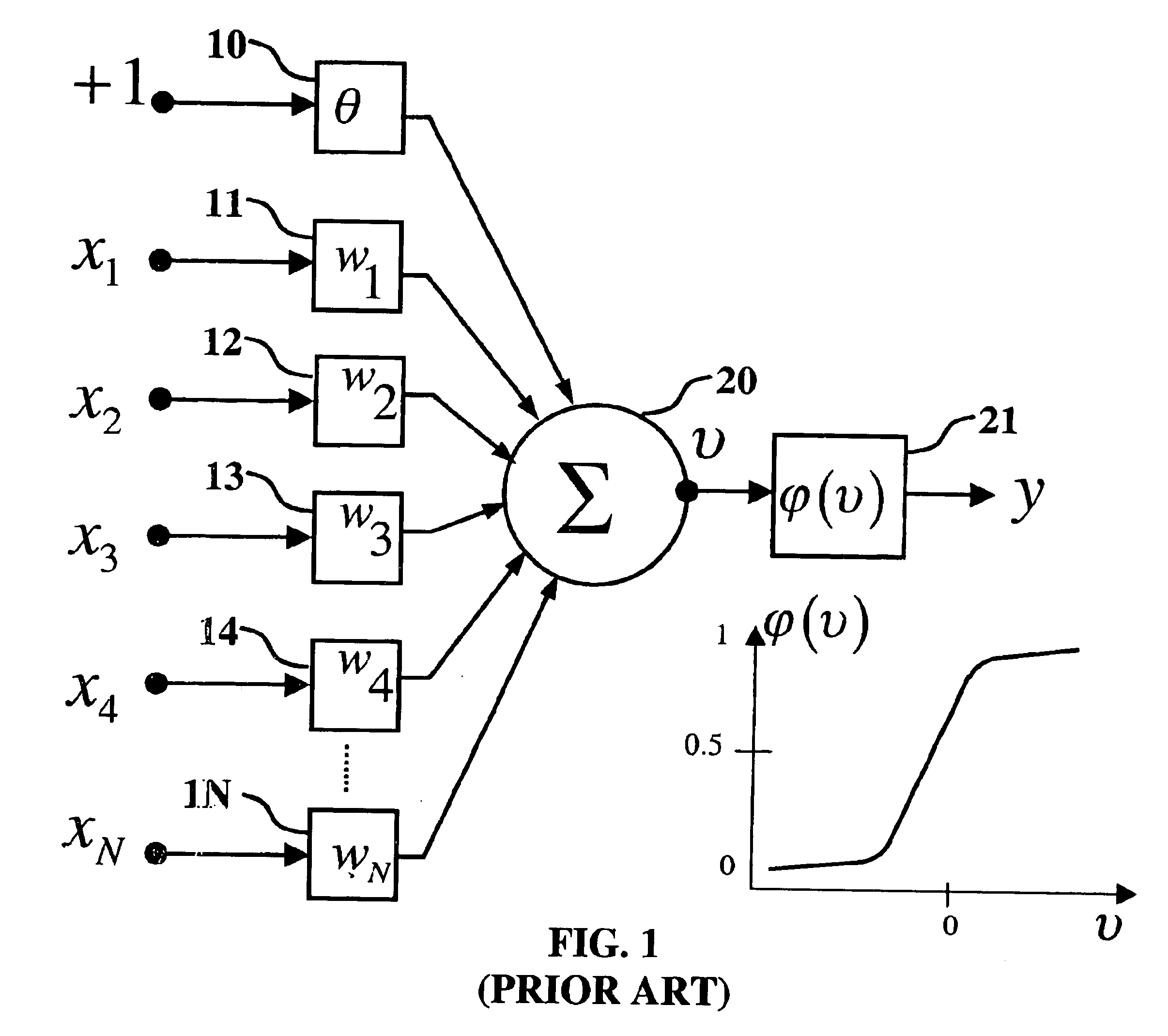
The well-known in the art input-output relation of the "linear combiner" (20), essential part of the computational model of a neuron with N-number of synapses shown on FIG. 1 is given by: ##EQU1##

where x.sub.k is the k-th input vector component (representing pre-synaptic activity signal quantity for synapse k) and .upsilon. is the output of the linear combiner or so called "induced local field" or activation potential value. Synapse weights or strengths denoted with w.sub.k for each synapse k are shown on FIG. 1 as (11),(12) . . . (1N). Further, typically, such a model will have some type of limiting non-linear function (21) applied to limit neuron's output activity: ##EQU2##

Since ...


PUM


Abstract

A method and apparatus for modeling a neural synapse function in analog hardware whereby the multiplication function inherent to the operation of a neural synapse is computed by applying a voltage on the gate-source terminals and an independent voltage on drain-source terminals of a MOSFET further using the resultant drain current of the latter device in non-saturation mode as function implementing a computation essentially close to multiplication function between the aforesaid voltages. Analog circuit is provided, capable of generating an output current signal which is proportional in magnitude, within a certain range, to a function computing essentially a sum of weighted input signals-products of corresponding pair of current input signal, and voltage control signal applied to a plurality of inputs thus capable of constructing an artificial neuron model.

Description

Not ApplicableReference to a "Microfiche Appendix"Not Applicable1. Field of the InventionThe present invention relates to modeling the function of a neural synapse in hardware thus allowing for building of neural networks or alike learning and adaptive systems using low-power conventional MOSFETs integrated on-chip with other analog or digital application circuits.2. Description of the Related and Prior ArtIn spite of the immense advance in the development of the modem VLSI technology, digital circuits or systems reach the critical point from its computational speed and integration. In implementing real-time digital signal processing applications, the conventional VLSI technology has many limitations with regard to chip area and its speed, due to complexity of both hardware and software processing algorithms. On the other hand, artificial neural networks offer great potential in many applications. This poses the need of a simple, fast and efficient solution for implementation of suc...

Claims


Application Information

Patent Timeline
Patent Type & Authority Patents(United States)
IPC IPC(8): G06N3/00G11C11/56G06N3/063
CPCG06N3/063G11C11/56G11C11/54
Inventor MILEV, MOMTCHIL MIHAYLOV
Owner TEXAS INSTR INC
Why Eureka
Try Eureka