Magnetic switching device and magnetic memory using the same

a switching device and magnetic memory technology, applied in the field of magnetic switching devices and magnetic memory using the same, can solve the problems of low energy conversion efficiency and achieve the effect of enhancing the energy conversion efficiency of changing

Active Publication Date: 2005-01-04
PANASONIC CORP
View PDF2 Cites 22 Cited by
  • Summary
  • Abstract
  • Description
  • Claims
  • Application Information

AI Technical Summary

Benefits of technology

Therefore, with the foregoing in mind, it is an object of the present invention to provide a magnetic switching device capable of enhancing an energy conversion efficiency for cha

Problems solved by technology

However, such a magnetic switching device has a problem of a low energy conversion efficiency as described below, and hence, the

Method used


Image

  • Magnetic switching device and magnetic memory using the same
  • Magnetic switching device and magnetic memory using the same
  • Magnetic switching device and magnetic memory using the same

Examples


example 1

A magnetic switching device (Sample 1) having the following film configuration was produced, using MBE. Sample 1 had the shape as shown in FIG. 12.

Sample 1

Sapphire substrate / AlN (500) / AlN:Si (100)AlMnN:Si (10) / CoFe (10) / AlO (1) / CoFe (10) / PtMn (25) / Ta (3) / Cu (100) / Ta (25)

Herein, the numerical values in the parentheses represent a film thickness. The unit is “nm”. Hereinafter, the film thickness will be shown similarly.

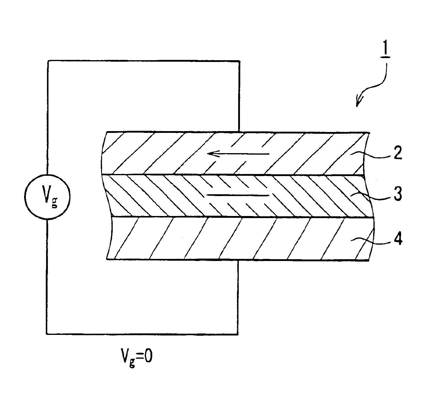
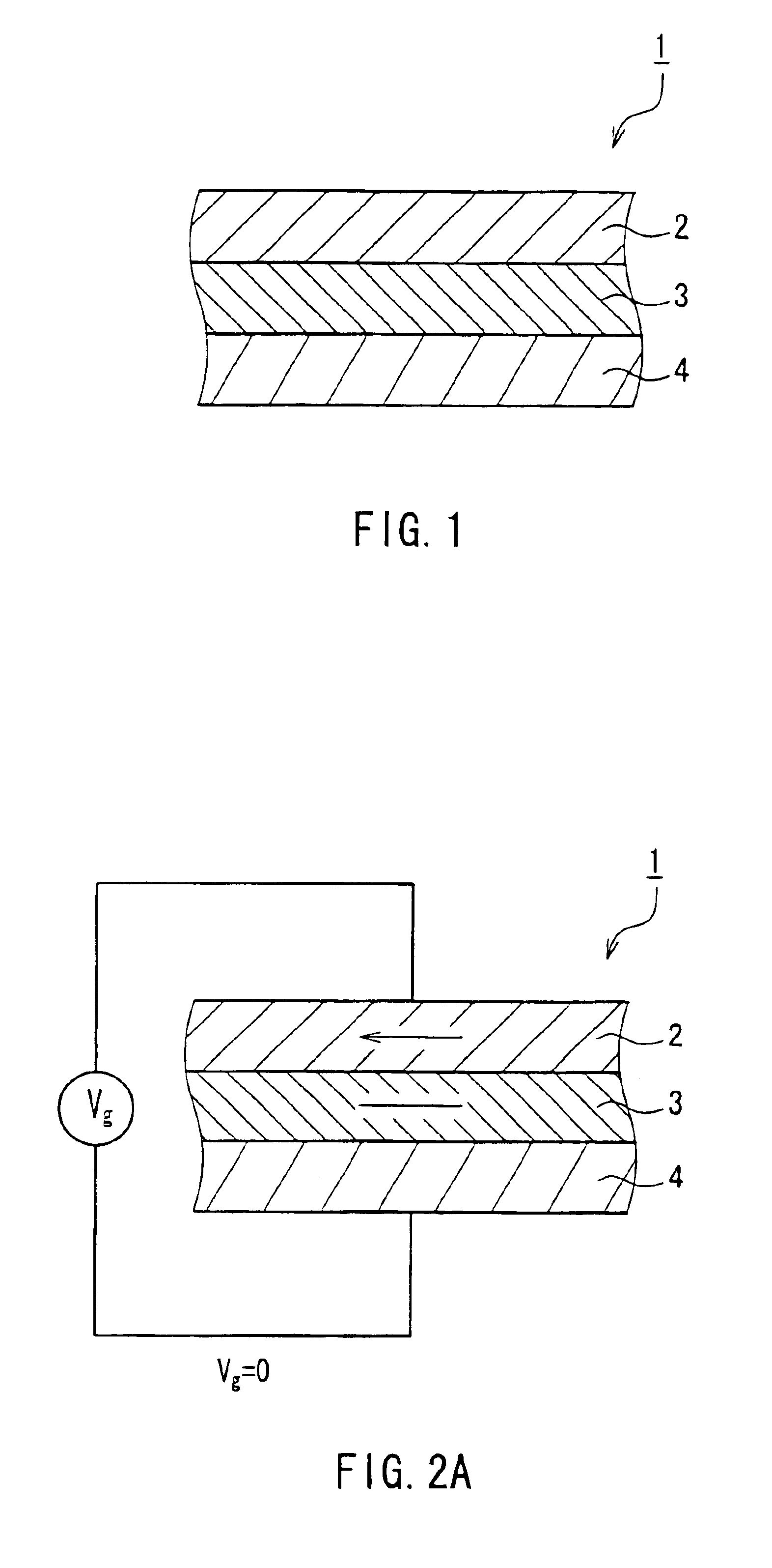
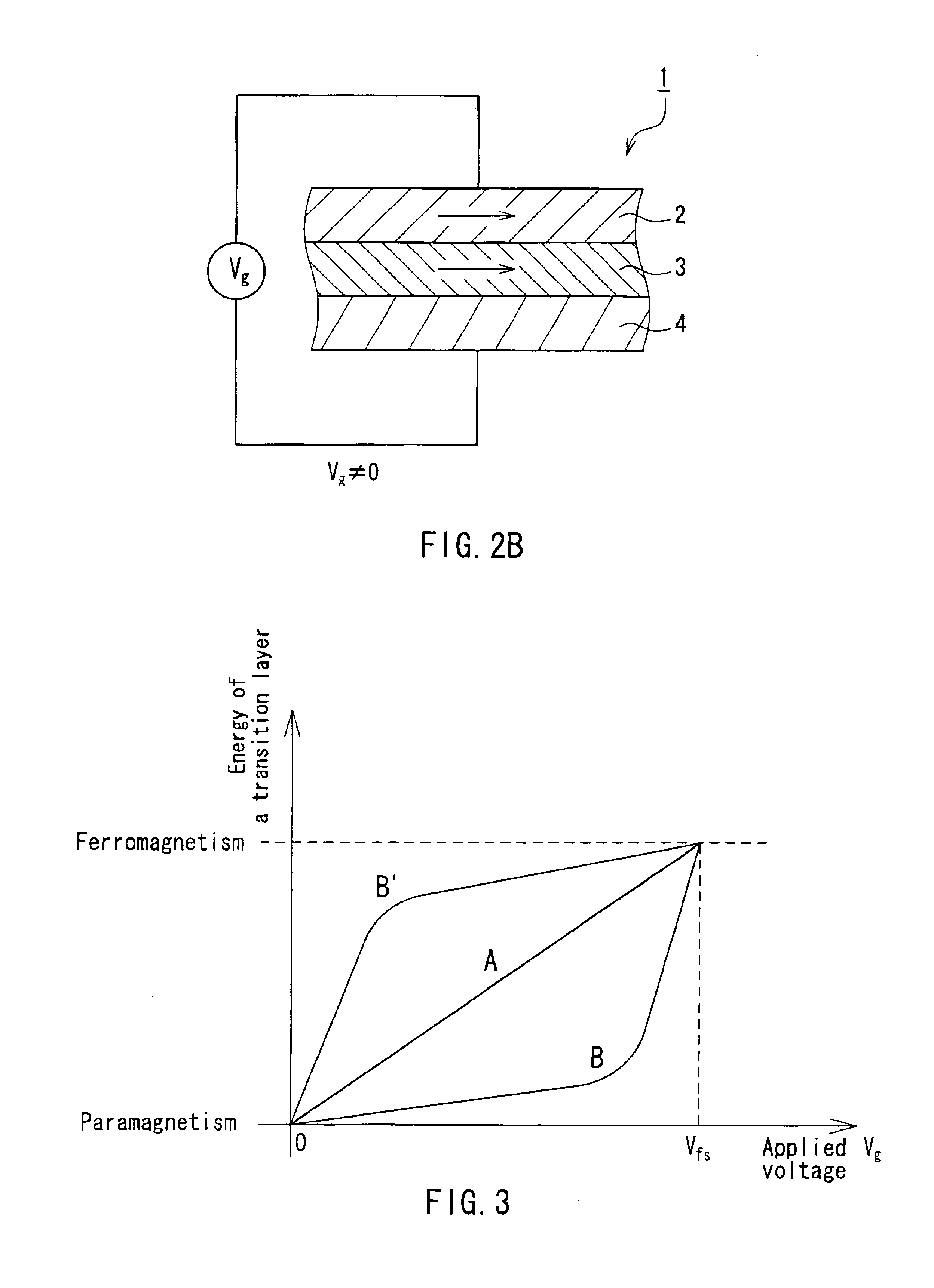
An AlN layer on the sapphire substrate is an insulating layer 7. An AlN:Si layer is a carrier supplier 4. An AlMnN:Si layer is a transition layer 3. A CoFe layer is a magnetic layer 2. AlO is a non-magnetic layer 15. A CoFe / PtMn layer is a fixed magnetic layer 16 with an anti-ferromagnetic substance (PtMn) laminated on CoFe. The PtMn layer made of an anti-ferromagnetic substance sets the adjacent CoFe layer to be a fixed magnetic layer by magnetic coupling. A Ta / Cu / Ta laminate is an electrode 6 on the fixed magnetic layer 16. This also applies to the other electrodes 6....

example 2

In Example 2, magnetic memories as shown in FIGS. 13 and 15 were produced using the magnetic switching device (Sample 1) produced in Example 1, and the characteristics thereof were evaluated. As a substrate, a CMOS substrate was used, and devices were arranged in a total of 8 blocks each having 16×16 devices.

Magnetic switching devices having a film configuration of Sample 1 were produced on a CMOS substrate in the same way as in Example 1. First, FETs were placed in a matrix as switching devices on a CMOS substrate. An interlayer insulating film was placed on the FETs to flatten the surface by CMP. Thereafter, the magnetic switching devices of Sample 1 were placed in a matrix so as to correspond to the FETs. After the magnetic switching devices were placed, hydrogen sintering treatment was performed at 400° C. One device in each block was set to be a dummy device for canceling a wiring resistance, a device minimum resistance, an FET resistance, and the like. Furthermore, word lines,...

example 3

A magnetic switching device (Sample 2) having the following film configuration was produced using pulse laser deposition (PLD). Sample 2 had the shape as shown in FIG. 12.

Sample 2

Sapphire substrate / AlN (500) / AlN:Si (100) / AlCoN:Si (10) / NiFe (10) / AlO (1) / CoFe (10) / PtMn (25) / Ta (3) / Cu (100) / Ta (25)

An AlN layer on the sapphire substrate is an insulating layer. An AlN:Si layer is a carrier supplier. An AlCoN:Si layer is a transition layer. An NiFe layer is a magnetic layer. AlO is a non-magnetic layer. A CoFe / PtMn layer is a fixed magnetic layer with an anti-ferromagnetic substance (PtMn) laminated on CoFe. The PtMn layer made of an anti-ferromagnetic substance sets the adjacent CoFe layer to be a fixed magnetic layer by magnetic coupling. A Ta / Cu / Ta laminate is an electrode on the fixed magnetic layer. This also applies to the other electrodes. An alignment constant of the sapphire substrate is (0001).

A method for producing Sample 2 will be described.

First, an AlN layer was produced on ...


PUM


Abstract

A magnetic switching device is provided, which has a configuration different from that of a conventional example and is capable of enhancing an energy conversion efficiency for changing the magnetized state of a magnetic substance. A magnetic memory using the magnetic switching device also is provided The magnetic switching device includes a magnetic layer, a transition layer magnetically coupled to the magnetic layer, and a carrier supplier including at least one selected from metal and a semiconductor. The transition layer and the carrier supplier are placed in such a manner that a voltage can be applied between the transition layer and the carrier supplier. The transition layer undergoes a non-ferromagnetism—ferromagnetism transition by the application of a voltage, and the magnetized state of the magnetic layer is changed by the transition of the transition layer.

Description

BACKGROUND OF THE INVENTION1. Field of the InventionThe present invention relates to a magnetic switching device and a magnetic memory using the same.2. Description of the Related ArtMagnetic switching devices including a magnetic substance, for performing conversion between electric energy and magnetic energy, are used for various magnetic devices such as a reproducing head of a magnetic recording apparatus, sensors (e.g., a force sensor, an acceleration sensor, etc.), and magnetic solid memories (e.g., a magnetic random access memory, etc.). However, such a magnetic switching device has a problem of a low energy conversion efficiency as described below, and hence, there is a demand for a magnetic switching device with a higher energy conversion efficiency (i.e., with reduced power consumption).As a method for controlling a magnetic switching device, for example, the magnetized state of a magnetic substance included in a magnetic switching device is changed, and as a more specific ...

Claims


Application Information

Patent Timeline
IPC IPC(8): G11C11/15H01F10/10H01L29/66G11C11/02H01L29/82H01F10/18H01L43/08G11B5/39H01F10/193H01L21/8246H01L27/22
CPCB82Y10/00B82Y25/00G11B5/3909H01F10/1936H01L27/228H01L29/82H01L43/08G11C11/15G11B5/3903G11B2005/3996H01F1/405H10B61/22H10N50/10
Inventor ODAGAWA, AKIHIROMATSUKAWA, NOZOMUSUGITA, YASUNARI
Owner PANASONIC CORP
Why Eureka
Try Eureka