Eureka AIR delivers breakthrough ideas for toughest innovation challenges, trusted by R&D personnel around the world.

Method for producing a phase shift mask

Inactive Publication Date: 2005-01-11
POLARIS INNOVATIONS
View PDF3 Cites 4 Cited by
  • Summary
  • Abstract
  • Description
  • Claims
  • Application Information

AI Technical Summary

Benefits of technology

A particular advantage of the present invention results from the fact that there is no need to carry out an additional deposition, exposure or novel etching process in order to carry out the method according to the invention. There is merely a need for two short additional chromium etching processes, as will be described in more detail in further aspects.
results from the fact that there is no need to carry out an additional deposition, exposure or novel etching process in order to carry out the method according to the invention. There is merely a need for two short additional chromium etching processes, as will be described in more detail in further aspects.
In a further configuration of the invention, the first chromium etching depth is fixed by a predefined first etching time. This measure ensures that, in a substantially reproducible method, a substantially constant thickness of the chromium layer is always left in the regions that are to be structured. According to a further configuration, the thickness is preferably between 5 and 20 nanometers. Starting from an initial chromium layer thickness of 100 nanometers—future high-specification mask blanks are anticipated to have thicknesses of only 70 nanometers—it is even now possible to achieve an accuracy of this level given a predetermined time and a constant etching rate.
The time control is preferably determined and defined experimentally in advance. It is substantially determined from the abovementioned initial chromium thickness and the etching rate. The homogeneity and isotropy or anisotropy of the etching process using a mask must also be taken into account. Criteria for the chromium thickness of the remaining layer in the structured region which can be achieved and have sufficient conductivity, which must be matched to the intensity and diameter of the electron or ion beam, and the optical transparency in order for it to be possible to carry out metrology and defect inspections between individual process steps, in particular between the planar exposures. This ensures that any repairs to the structures can be carried out, for example the application of chromium.
In the case of high-quality etching equipment which is currently in use, the accuracy for the formation of a residual chromium thickness during time-controlled etching is approximately 5 nanometers.
In a further configuration of the present invention, after structuring of the second level, i.e. a second exposure by electron or ion beam, a chromium etching step is carried out, which etches away the remaining, reduced chromium layer in the structured regions of the second level. In a further configuration, which preferably relates to alternating phase shift masks, the etching step is also carried out in a time-controlled manner, in order advantageously not to obtain any unreliable signals as a result of the chromium edges of the solid, initial chromium thickness which in this case project within the structure holes in the resist layer which is still present. When the same etching process as in the first etching step is used, the duration of the second chromium etching will be substantially proportional to the first duration.

Problems solved by technology

The premature interruption to the etching step is caused by a thin film of the chromium layer being left between the chromium regions which may otherwise be isolated.

Method used


Image

  • Method for producing a phase shift mask
  • Method for producing a phase shift mask
  • Method for producing a phase shift mask

Examples


Embodiment Construction

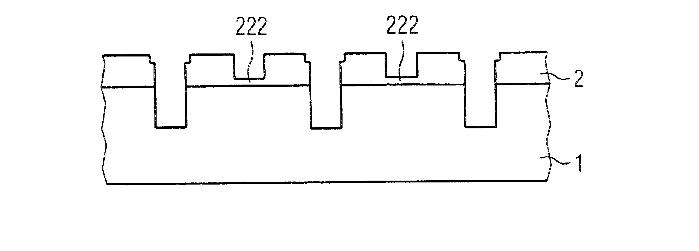
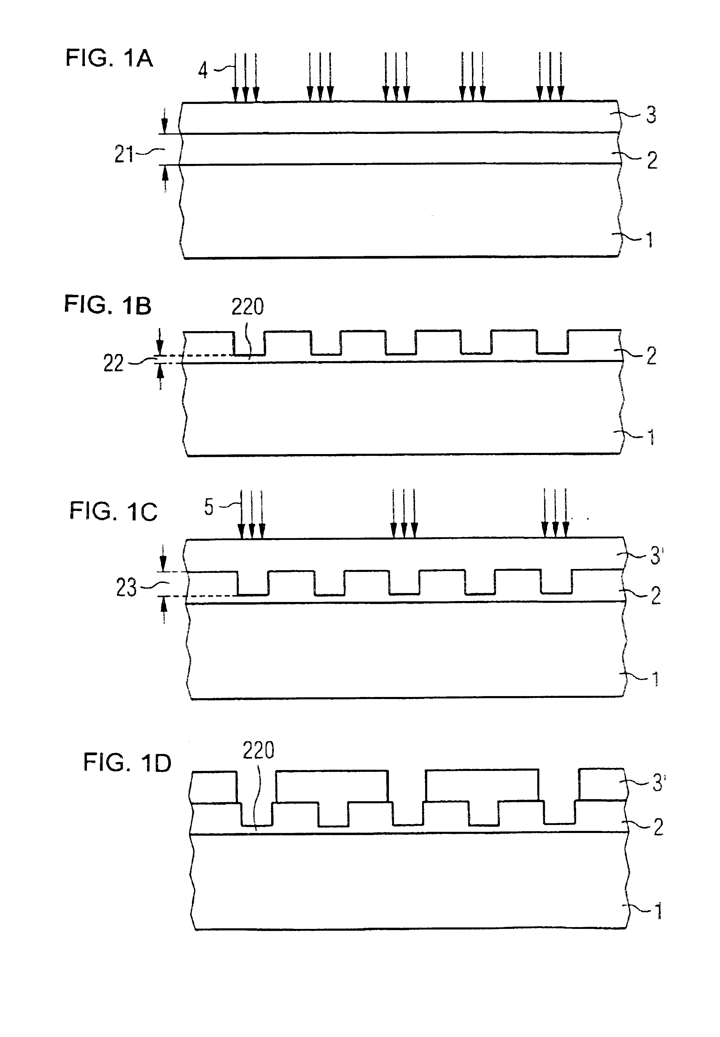
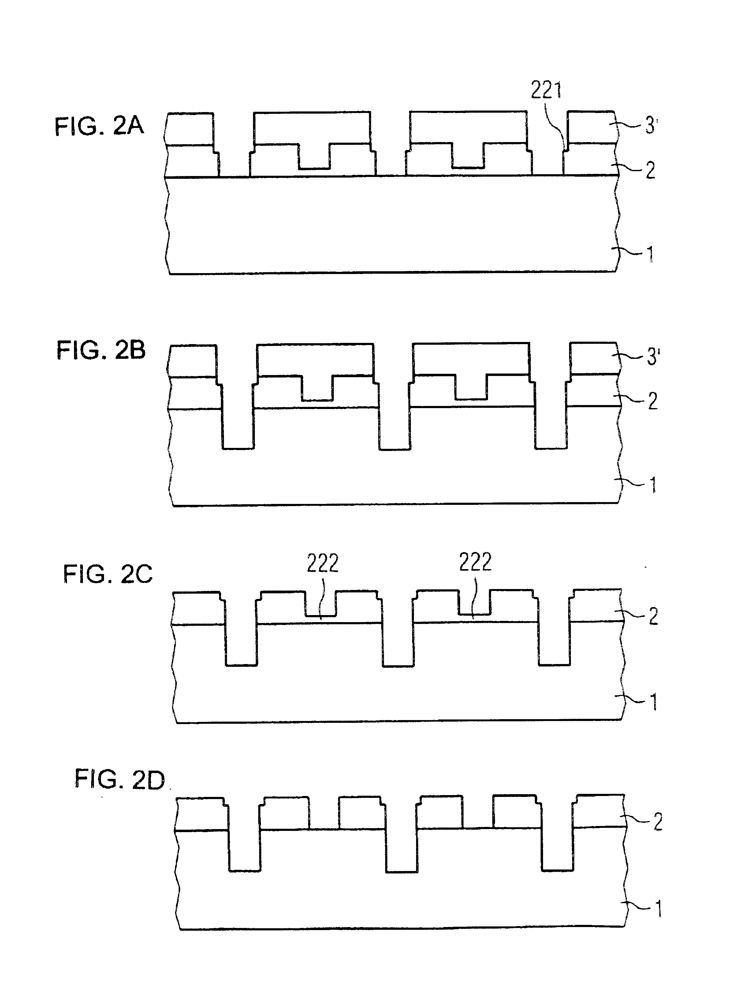
Referring now to the figures of the drawing in detail and first, particularly, to FIGS. 1A-1D thereof, there are shown process steps of an inventive production process for alternating phase shift masks through to exposure and development of a second level. A quartz blank is provided as a transparent substrate material 1. The substrate material 1 is coated with a chromium layer 2 of an initial chromium thickness 21 and a charge-sensitive resist layer 3 above it. The transparent substrate material 1 is exposed by an electron beam 4 that has a row and column structure. After a developing step, a first chromium etching step is carried out, during which, after a predetermined, defined duration, the etching operation is terminated. The duration was determined experimentally for the plasma etching unit used in the present example and blanks with an initial chromium thickness 21 of 100 nm, in such a manner that, after the first chromium etching step, there is a residual chromium thickness 2...


PUM


Abstract

To avoid charging effects of isolated chromium structures during the structuring of a second level of attenuated phase shift masks, a previous chromium etching step is preferably carried out in a time-controlled manner, so that a residual chromium layer, which is approximately 5-20 nm thick, remains at the bottom of the columns. The residual chromium layer connects the chromium webs, which are otherwise isolated, in a conductive manner and therefore dissipates the charge to the outside during the subsequent structuring by an electron beam. In the process steps that follow the exposure of the second level—preferably of alternating attenuated phase shift masks—two further chromium etching steps can be carried out, with a small etching depth in each case in the columns provided for the quartz etching of different phase shift.

Description

BACKGROUND OF THE INVENTIONField of the InventionThe present invention relates to a method for producing a phase shift mask.To transfer structures with a resolution of as little as a few tens of nanometers to silicon wafers or similar semiconductor products, it is customary to use masks, on which the structure which is to be transferred is present in binary form, for example linear regions covered by opaque chromium on an otherwise transparent substrate material, generally quartz. In the case of a projection carried out with optical wavelengths, the masks are transilluminated and the structures are transferred in an identical or reducing image, via a lens system, to the light-sensitive layer of a wafer. However, for future mask technologies, images produced via reflection on the mask surface will also be considered.The trend toward increasingly small feature sizes on the wafer imposes constantly increasing demands on the technology of the mask or the reticle for reducing projection,...

Claims


Application Information

Patent Timeline
IPC IPC(8): G03F1/00
CPCG03F1/30G03F1/26G03F1/0092
Inventor CRELL, CHRISTIAN
Owner POLARIS INNOVATIONS
Why Eureka
Eureka Blog
Learn More