Group III-V compound semiconductor and group III-V compound semiconductor device using the same

a compound semiconductor and semiconductor technology, applied in the direction of semiconductor lasers, basic electric elements, lasers, etc., can solve the problems of large number of crystal defects, difficult to realize a group iii-v compound semiconductor, and crystal defect density increase, so as to reduce the density of crystal defects

Inactive Publication Date: 2005-01-11
PANASONIC CORP
View PDF3 Cites 56 Cited by
  • Summary
  • Abstract
  • Description
  • Claims
  • Application Information

AI Technical Summary

Benefits of technology

In this way, it is possible to reduce the crystal defect density at the interface between the first semiconductor layer or the second semiconductor layer and the buffer layer while the buffer layer gives substantially no influence on the electrical and optical characteristics of the group III-V compound semiconductor device.

Problems solved by technology

However, the group III-V compound semiconductor is observed, with human eyes, to be cloudy across the entire surface thereof, indicating occurrence of crystal defects.
As described above, when a group III-V compound semiconductor is produced in which an AlGaAs layer is deposited on an AlGaInP layer, a large number of crystal defects occur.
Therefore, it is difficult to realize a group III-V compound semiconductor, or a group III-V compound semiconductor device using the same, in which an AlGaAs layer is deposited on an AlGaInP layer.

Method used


Image

  • Group III-V compound semiconductor and group III-V compound semiconductor device using the same
  • Group III-V compound semiconductor and group III-V compound semiconductor device using the same
  • Group III-V compound semiconductor and group III-V compound semiconductor device using the same

Examples


first embodiment

The first embodiment of the present invention will now be described with reference to the drawings.

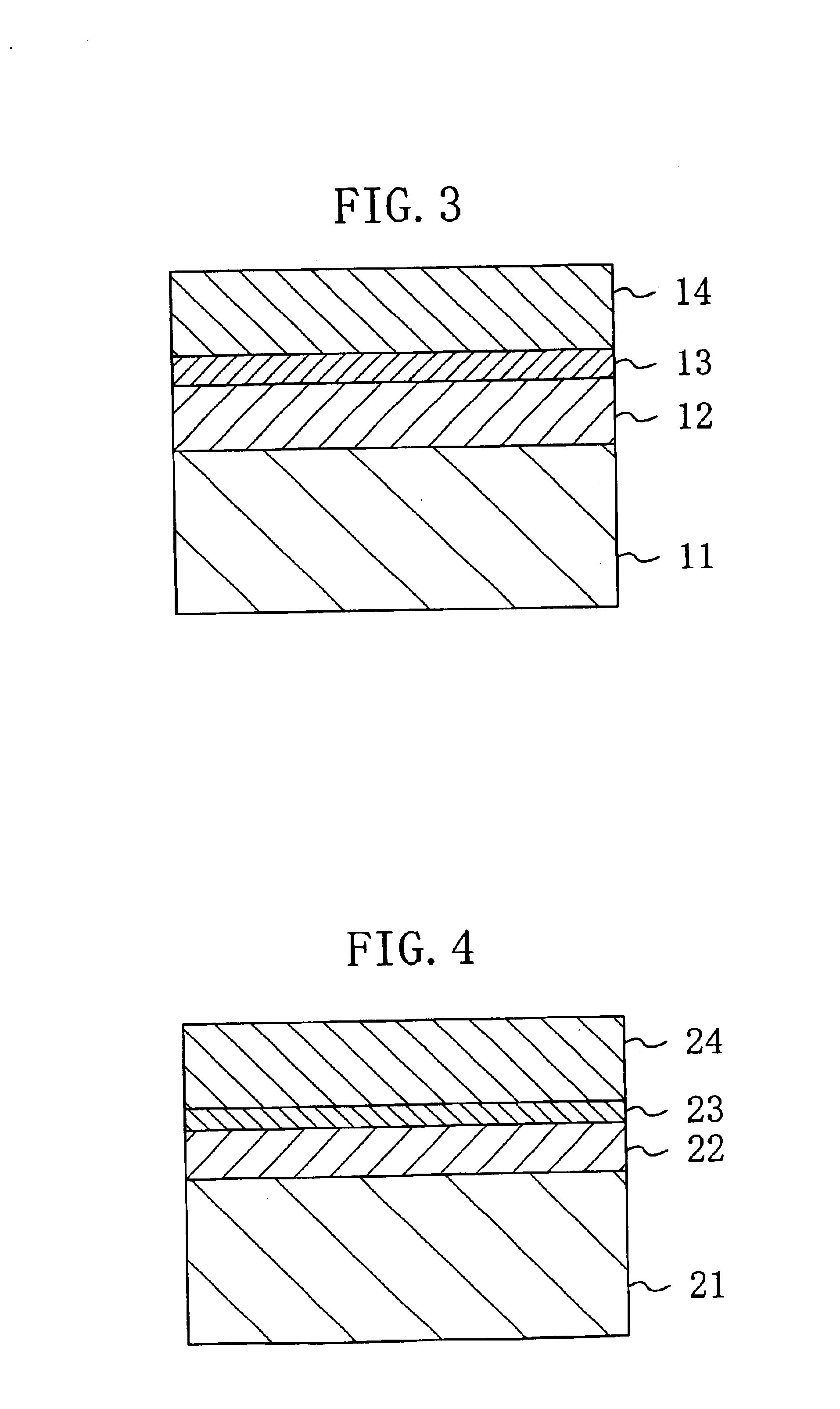
FIG. 3 is a cross-sectional view illustrating a group III-V compound semiconductor layered structure according to the first embodiment. As illustrated in FIG. 3, an AlGaInP layer 12 made of Al0.35Ga0.15In0.5P having a thickness of about 0.2 μm, a buffer layer 13 made of Al0.5In0.5P having a thickness of about 1.1 nm, and an AlGaAs layer 14 made of Al0.6Ga0.4As having a thickness of about 0.3 μm, are deposited in this order on a substrate 11 made of GaAs, for example.

A method for manufacturing the group III-V compound semiconductor layered structure of the first embodiment will now be described.

The group III-V compound semiconductor layered structure of the first embodiment can be formed by successively growing the semiconductor layers on the substrate 11 made of GaAs by using an MOVPE method, for example.

Specifically, triethylgallium (TEG), trimethylaluminum (TMA) and trimethylindium (...

second embodiment

The second embodiment of the present invention will now be described with reference to the drawings.

FIG. 4 is a cross-sectional view illustrating a group III-V compound semiconductor layered structure according to the second embodiment. As illustrated in FIG. 4, an AlGaInP layer 22 made of Ga0.5In0.5P having a thickness of about 30 nm, a buffer layer 23 made of GaAs having a thickness of about 1.6 nm, and an AlGaAs layer 24 made of Al0.6Ga0.4As having a thickness of about 0.3 μm, are deposited on a substrate 21 made of GaAs.

Such a group III-V compound semiconductor layered structure can be formed by using an MOVPE method, for example, as in the first embodiment.

A feature of the second embodiment is that the AlGaAs layer 24 is formed on the AlGaInP layer 22 via the buffer layer 23 made of AlGaAs, and the Al content in the buffer layer 23 is smaller than that in the AlGaAs layer 24. Thus, instead of depositing the AlGaAs layer 24 made of Al0.6Ga0.4As directly on the AlGaInP layer 22, ...

third embodiment

A semiconductor laser device according to the third embodiment will now be described with reference to the drawings.

FIG. 5 is a cross-sectional view illustrating the semiconductor laser device according to the third embodiment of the present invention. As illustrated in FIG. 5, an n-type cladding layer, 32 made of n-type AlGaInP, an active layer 33 including a multiple quantum well and optical guiding layers interposing the multiple quantum well therebetween, a buffer layer 34 made of AlGaInP, a dopant diffusion preventing layer 35 made of AlGaAs, and a first p-type cladding layer 36 made of p-type AlGaInP, are deposited in this order on a substrate 31 made of n-type GaAs.

Note that in the active layer 33, the multiple quantum well has an alternating pattern of three well layers made of GaInP and two barrier layers made of AlGaInP, with two of the well layers being the outermost layers of the multiple quantum well, and an optical guiding layer made of AlGaInP is formed on the upper s...


PUM


Abstract

An AlGaInP layer is formed on a substrate made of GaAs, and an AlGaAs layer is formed on the AlGaInP layer via a buffer layer therebetween. The buffer layer has a thickness of about 1.1 nm and is made of AlGaInP whose Ga content is smaller than that of the AlGaInP layer. The buffer layer may alternatively be made of AlGaAs whose Al content is smaller than that of the AlGaAs layer.

Description

BACKGROUND OF THE INVENTIONA group III-V compound semiconductor is widely used as a material of various semiconductor elements such as a light emitting element, e.g., a semiconductor laser diode (LD) and a light emitting diode (LED), and a logic circuit element, e.g., a field effect transistor (FET) and a heterojunction bipolar transistor (HBT). In these devices, a plurality of semiconductor layers having different mixed crystal compositions are layered together to realize intended optical and electrical characteristics.A semiconductor device made of such a group III-V compound semiconductor requires a thickness control on the nanometer order and an interface steepness, and is thus typically manufactured by using a metal organic vapor phase epitaxy (MOVPE) method or a molecular beam epitaxy (MBE) method.Particularly, AlxGayIn1−x−yP (where 0≦x≦1, 0≦y≦1, 0≦x+y≦1) and AlzGa1−zAs (where 0≦z≦1), which have band gaps corresponding to the visible region and the infrared region, respectivel...

Claims


Application Information

Patent Timeline
Patent Type & Authority Patents(United States)
IPC IPC(8): H01L21/02H01L21/20H01L29/02H01L29/201H01L29/205H01L33/00H01L33/30
CPCH01L21/02392H01L21/02395H01L21/02461H01L21/02502H01L33/30H01L21/02546H01L21/0262H01L29/201H01L29/205H01L21/02543
Inventor ONISHI, TOSHIKAZU
Owner PANASONIC CORP
Why Eureka
Try Eureka