Chip-like electronic components, a method of manufacturing the same, a pseudo wafer therefor and a method of manufacturing thereof

a technology of electronic components and manufacturing methods, applied in semiconductor/solid-state device testing/measurement, semiconductor devices, semiconductor/solid-state device details, etc., can solve the problems of increased thickness of stacked packages, easy cracking, and low yield of production resulting from increased processing steps, so as to facilitate handling and reduce thickness , the effect of excellent package reliability

Inactive Publication Date: 2005-01-11
SONY CORP
View PDF30 Cites 15 Cited by
  • Summary
  • Abstract
  • Description
  • Claims
  • Application Information

AI Technical Summary

Benefits of technology

According to the present invention, because the side surfaces of the chip-like electronic component such as the semiconductor chip or the like (hereinafter explained by referring to the semiconductor chip such as LSI chip) other than its electrode surface are protected with a protective material, the chip is ensured to be protected in its post chip handling using such as a collet, thereby facilitating its handling and enabling an excellent package reliability to be obtained. In addition, because the bottom surface of the electronic component (opposite to the electrode surface) is fabricated to reduce its thickness, an improved stack (lamination) packaging density due to a thinner structure is attained advantageously.
Further, by the method comprising the steps of: pasting on a substrate solely non-defective chips which are diced and selected from a semiconductor wafer; coating them wholly with the protective material, though a part of them is removed by grinding afterward; then peeling the wafer bonding these chips from the adhesive material, a pseudo wafer of the present invention as if comprising entirely of the non-defective chips is obtained. Therefore, a wafer batch bump treatment for these non-defective chips becomes possible, thereby allowing to form bump chips at a lower cost, and when dicing these chips from the pseudo wafer, the portion of the protective material which is easy to cut and placed between adjacent chips is cut along the scribe line thereby without causing any adverse effect (such as strain, burr, crack and the like damages) to occur on the body of these chips. In addition, because the side surfaces of these chips are coated with the protective material, an Ni electroless plating process can be executed as well. Further, not only in-house produced wafers but also bare chips purchased from the other manufacturers are allowed to be treated likewise to form the solder bump easily.
By the way, it is very rare that all of a plurality of different types of LSI chips to be packaged in an MCM are supplied from a same semiconductor manufacturer because of an increasing burden to invest on several leading edge semiconductor production lines simultaneously. Therefore, by opting not to purchase a whole bunch of chips of SRAMs, flash memories, microcomputers or even central processor units (CPUs) from the same semiconductor manufacturer, but to purchase them individually from different chip manufacturers who are most specialized in any one of these leading-edge technologies, they can be assembled in an MCM according to the present invention. In addition, the substrate described above can be used in repetition advantageously for cost reduction of bump forming and for environmental protection.
Namely, a novel process is provided according to the present invention, the same comprising the steps of: pasting a plurality (of a same type) and / or different types of LSI chips, for example, on a quartz substrate, apart from each other at a predetermined distance, with their device surfaces facing down; coating with an insulating material (such as a resin, SiOx by SOG (spin on glass)) from the bottom side of the chips, and hardening the same; reducing a total thickness by grinding or the like; and removing the pseudo wafer from the substrate, with the periphery of these chips thereon being protected by the insulating material. Thereby, this novel process of the invention enables readily to provide a method of fabricating thinner type chip components featuring a minimal damage, and an easier handling thereof.
Further, in the above-mentioned processing, the damage (such as stress, crack and the like) hardly remains even if the semiconductor chip is fabricated thinner. Further, a mechanical impact exerted on the body of the chip during packaging handling or the like is mitigated because that the sidewalls of the chip are covered with and protected by the protective material. Still further, because that respective side walls of respective chips are bonded integrally with the insulating film, there is no need of applying a chemical etching process after the grinding process as required conventionally, thereby preventing the device surface of each LSI chip from being etched by a penetrating solution.
The above-mentioned substrate made of quartz or the like can be used repeatedly, which is very advantageous in terms of cost reduction and environmental protection.

Problems solved by technology

Conventional high density packaging technology has been challenging how to improve a surface packaging density mainly, and there have been many discussions on a more compact package design, chip scale packaging (CSP), a real chip size CSP using a flip chip connection, and a bare chip packaging technology.
Although FIG. 10C is a diagram showing an example of stacked packaging of semiconductor LSIs via a plurality of interposers 60, there is a problem that as the number of stacked semiconductor LSIs increases, a height of a stacked package increases.
By way of example, there is a problem that a crack tends to occur easily when the thickness of the LSI chip 65 which was ground becomes thinner at the time of dicing of the LSI wafer 61.
Also, a low yield in production resulting from the increased steps of processing is a serious problem which cannot be ignored.
However, it has a disadvantage when being applied to the processing of a leading-edge wafer 61 which normally has a low yield of production, and because a cost of production per non-defective chip 30 will substantially increase.
Further, there has been such a problem that if bare chips are purchased from the other manufacturers or venders, it is extremely difficult to form bumps on them due to a varied design specification.
Namely, although the above-mentioned two types of bump forming methods have their own merits, they cannot be used in all fields.
Further, when the semiconductor wafer 61 indicated in FIG. 9 is diced along the scribe line 70, a damage such as a stress or a crack occurs in the chip due to its dicing, which may lead to a failure.
Furthermore, if a process of forming solder bumps in batch on the semiconductor wafer 61 which includes both the conforming chips 30 and the defective chips 29 is allowed to proceed, the process applied to the defective chips 29 is wasted, thereby increasing the cost of manufacture.
According to this conventional method, although it is proposed that a wafer batch processing becomes possible and a low cost manufacture thereof by a merit of mass production is attained, however, because there exists a hard substrate made of alumina under the bottom surfaces of these semiconductor chips which are arrayed on the wafer, at the time of scribing and cutting into each dice, the hard substrate present under the bottom surfaces of the chips must be cut together with the resin between adjacent chips, thereby likely to damage a cutter blade.
In addition, although the side walls of the chip are covered with the resin, there exists only the hard substrate on the bottom surface thereof, therefore, there are such problems that the bottom surface of the chip is not protected effectively and adhesion therebetween is weak.
Further, a conventional grinding process for grinding the bottom surface of the wafer causes a grinding damage such as stress, crack and the like to arise after its mechanical processing.
Because this mechanical damage leads to an occurrence of chip cracks when mounting a very thin chip on a printed board and in its handling, a process of removal of a damaged layer by polishing or chemical etching becomes necessary after the mechanical grinding.
Therefore, if adhesion between a double-sided adhesion sheet and the device surface of the chip 4 is weak, there occurs a serious problem that the device surface is easily etched.
By the way, it is very rare that all of a plurality of different types of LSI chips to be packaged in an MCM are supplied from a same semiconductor manufacturer because of an increasing burden to invest on several leading edge semiconductor production lines simultaneously.
Further, in the above-mentioned processing, the damage (such as stress, crack and the like) hardly remains even if the semiconductor chip is fabricated thinner.

Method used


Image

  • Chip-like electronic components, a method of manufacturing the same, a pseudo wafer therefor and a method of manufacturing thereof
  • Chip-like electronic components, a method of manufacturing the same, a pseudo wafer therefor and a method of manufacturing thereof
  • Chip-like electronic components, a method of manufacturing the same, a pseudo wafer therefor and a method of manufacturing thereof

Examples


Embodiment Construction

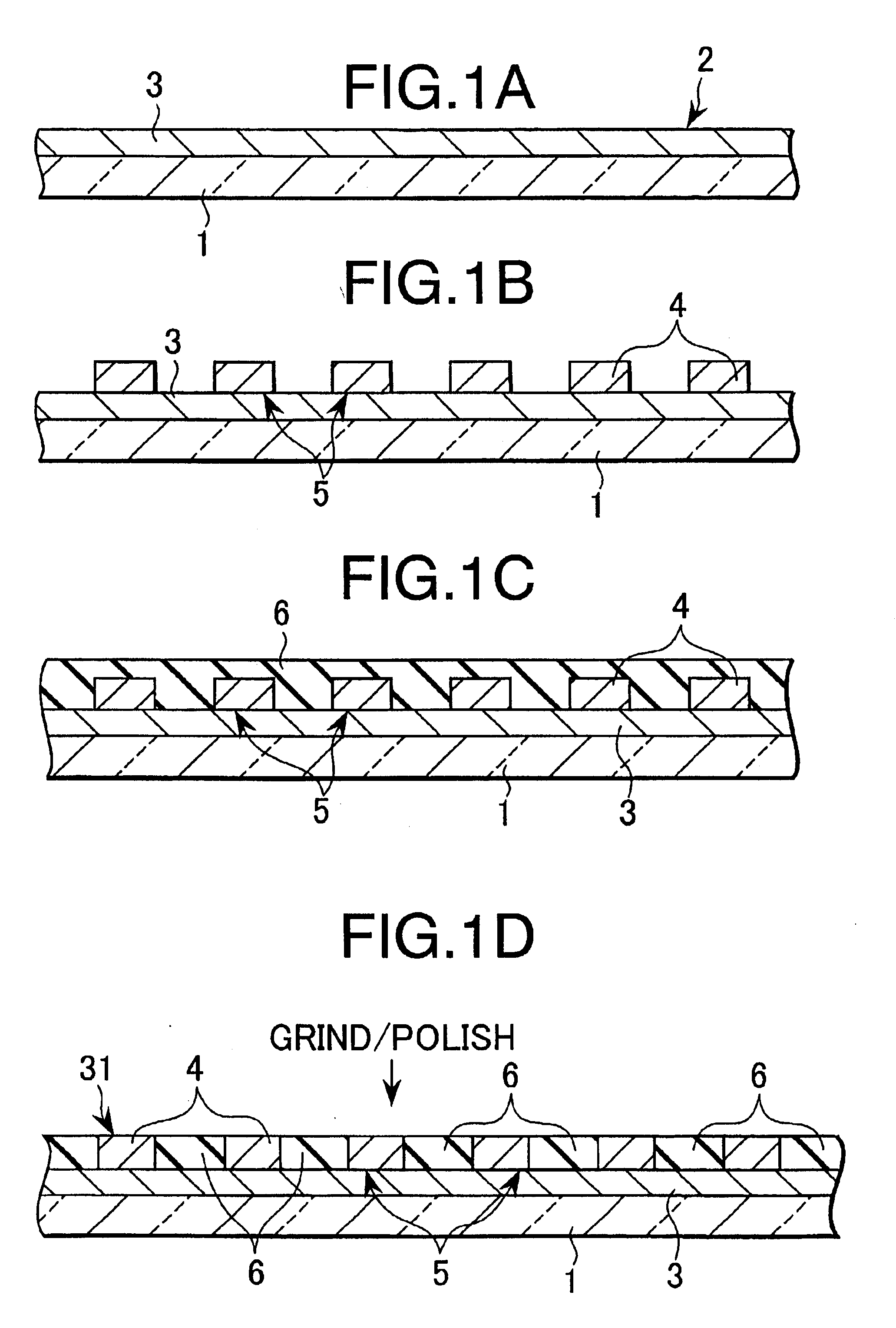
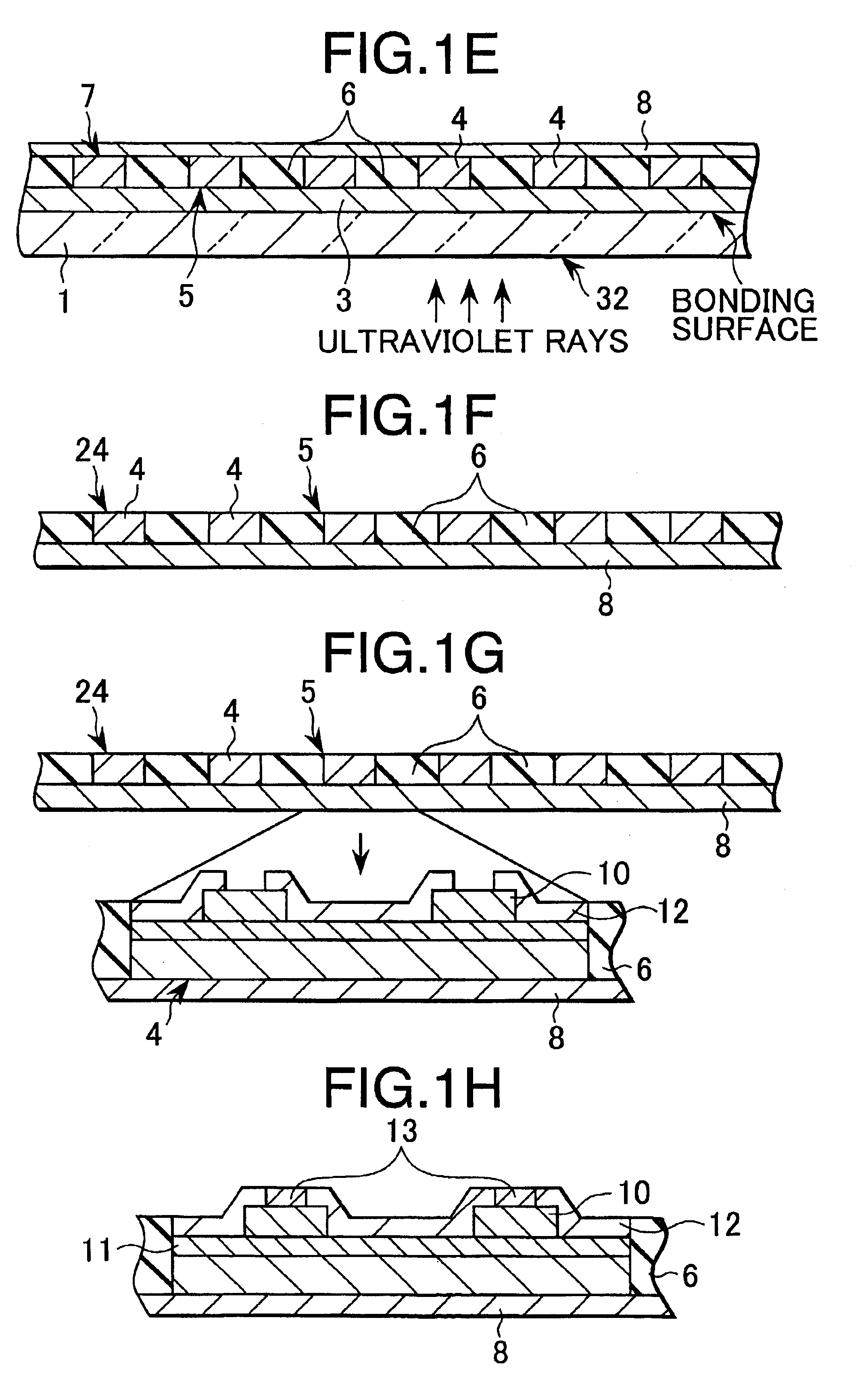
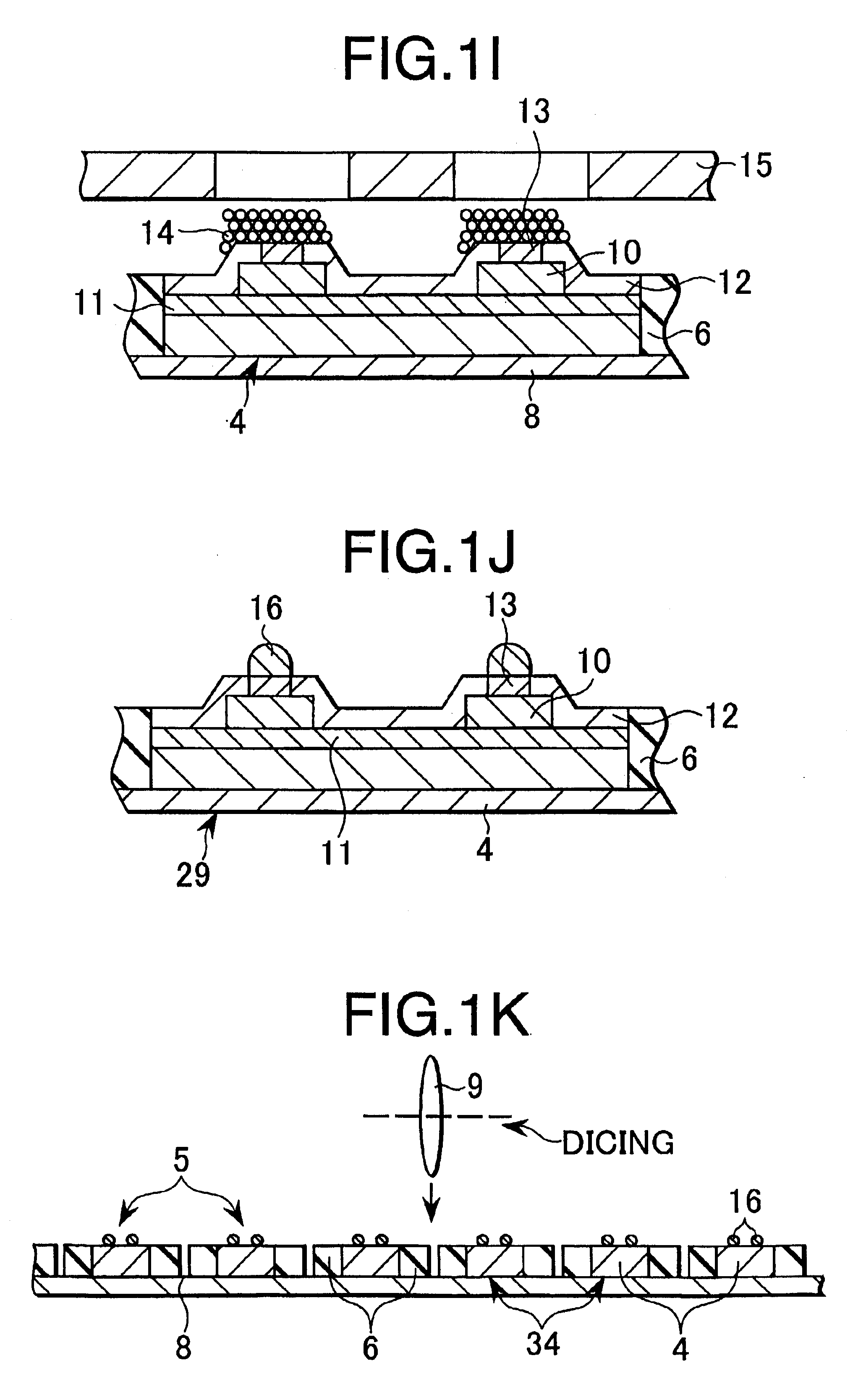
According to the present invention, the above-mentioned protective material is preferably an organic insulating resin or an inorganic insulating material. The semiconductor chip that is diced at the position of the aforementioned protective material and to be fixed on the package substrate (which chip may be a single chip or a plurality of the same or different types of chips integrated using the protective material) preferably has its device surface provided with the electrodes, its side walls covered with the protective material, and solder bumps formed on the electrodes.

Further, preferably, a single or a plurality of the same or the different types of integrated semiconductor chips to be mounted on a packaging substrate are provided by the steps of: pasting the adhesive sheet functioning as the above-mentioned adhesive material, on a flat transparent substrate or the like; fixing the plurality of the same or different types of semiconductor chips all of which are non-defective, o...


PUM


Abstract

In order to have a thin type semiconductor chips featuring a high yield and a low cost in production, an excellent packaging reliability, and a robust structure against damages, there is provided a method of manufacturing LSI chips, comprising the steps of: pasting on a substrate an adhesive sheet which retains its adhesive strength prior to a processing, then loses it after the processing; bonding non-defective LSI chips on the adhesive sheet, with their device surfaces facing downward; uniformly coating an insulating film on the non-defective LSI chips; uniformly grinding the insulating film to a level of the bottom surfaces of these LSI chips; applying a predetermined process to the adhesive sheet to weaken its adhesive strength thereof so as to peel off a pseudo wafer on which the non-defective LSI chips are bonded; and dicing the LSI chips into a discrete non-defective electronic component by cutting the pseudo wafer.

Description

RELATED APPLICATION DATAThe present application claims priority to Japanese Application No. P2000-130001 filed Apr. 28, 2000, which application is incorporated herein by reference to the extent permitted by law.BACKGROUND OF THE INVENTIONThe present invention relates to a chip-like electronic component suitable for use in the manufacture of a semiconductor device and a method of manufacturing the same, and in particular, it relates to a pseudo wafer for use in the manufacture of the same and a method therefor.Recently, in line with a recent growing demand for a more compact and lightweight design of electronic devices typically represented by a portable information terminal and the like, a very high density packaging technology for packaging semiconductor LSIs (large-scaled integration) in a limited space is attracting much attention.Conventional high density packaging technology has been challenging how to improve a surface packaging density mainly, and there have been many discuss...

Claims


Application Information

Patent Timeline
Patent Type & Authority Patents(United States)
IPC IPC(8): H01L23/31H01L23/28H01L21/68H01L21/67H01L25/10H01L21/301H01L21/56H01L21/66H01L23/12H01L25/04H01L25/065H01L25/18
CPCH01L21/561H01L23/3114H01L24/97H01L25/0657H01L21/568H01L2224/16225H01L25/105H01L2221/6834H01L2224/16145H01L2224/16227H01L2224/274H01L2224/32145H01L2224/32225H01L2224/48227H01L2224/97H01L2225/0651H01L2225/06517H01L2225/0652H01L2225/06572H01L2225/06586H01L2924/01004H01L2924/01013H01L2924/01015H01L2924/0103H01L2924/01033H01L2924/01075H01L2924/01078H01L2924/01079H01L2924/01082H01L2924/14H01L2924/15311H01L2924/1532H01L2924/15331H01L2924/10253H01L2924/01019H01L2924/01006H01L24/48H01L2924/01005H01L2924/00H01L2924/12042H01L2924/00015H01L2224/05001H01L2224/05022H01L2224/05571H01L2224/73204H01L2924/00014H01L2224/02166H01L24/73H01L2224/48091H01L2224/73207H01L2224/73265H01L2924/15321H01L2224/85399H01L2224/45099H01L2224/05599H01L2224/05541H01L2224/05005H01L2224/45015H01L2924/207H01L2924/00012H01L23/12
Inventor NISHIYAMA, KAZUO
Owner SONY CORP
Why Eureka
Try Eureka