

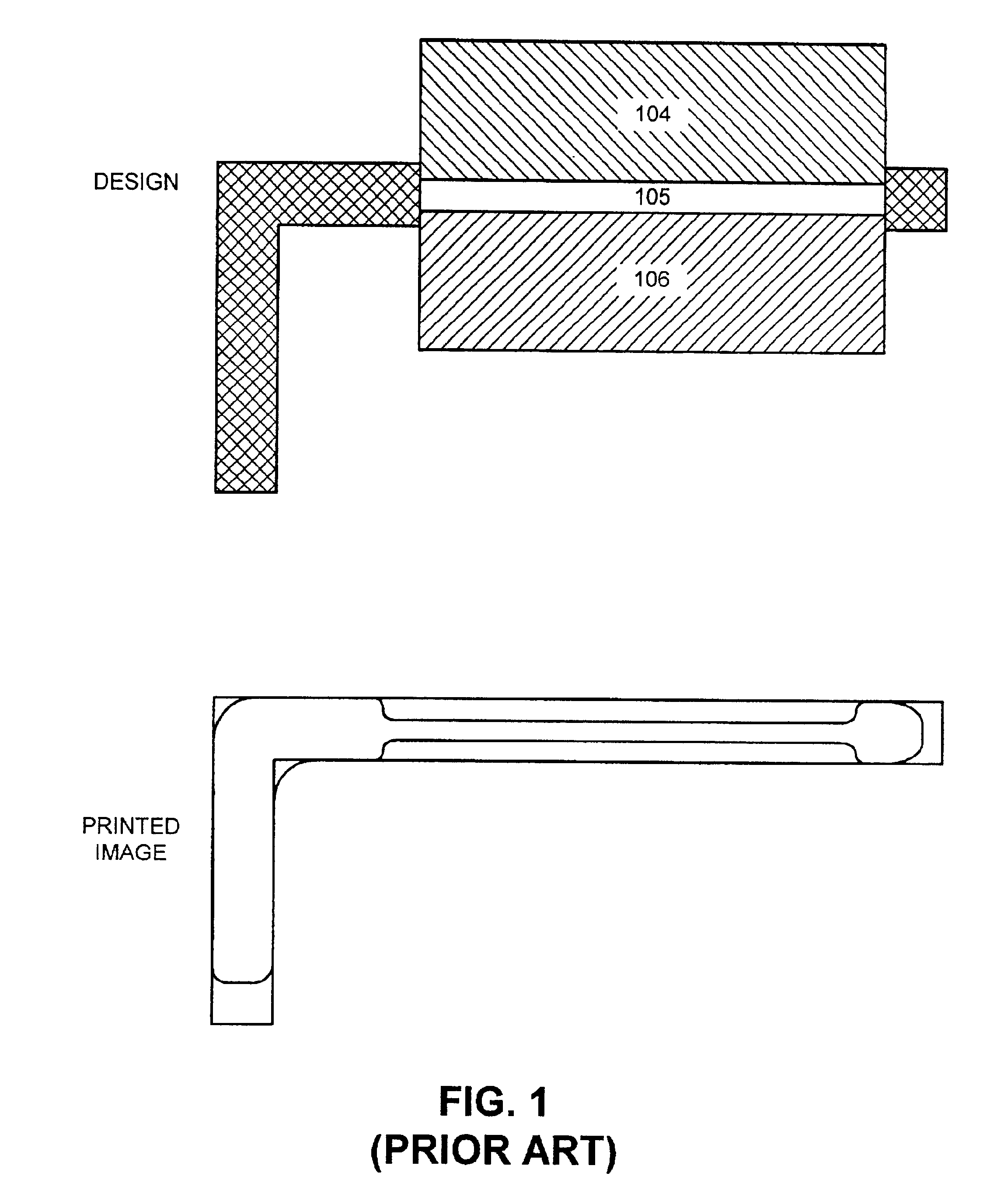
Facilitating optical proximity effect correction through pupil filtering
a technology of pupil filtering and optical proximity, which is applied in the field of manufacturing integrated circuits, can solve the problems of circuit designers being forced to deal, the edges of features deviating from desired locations, and the feature size of these circuit elements continues to decrease, so as to achieve the effect of mitigating optical proximity effects
- Summary
- Abstract
- Description
- Claims
- Application Information
AI Technical Summary
Benefits of technology
Problems solved by technology
Method used
Image

Examples
Embodiment Construction
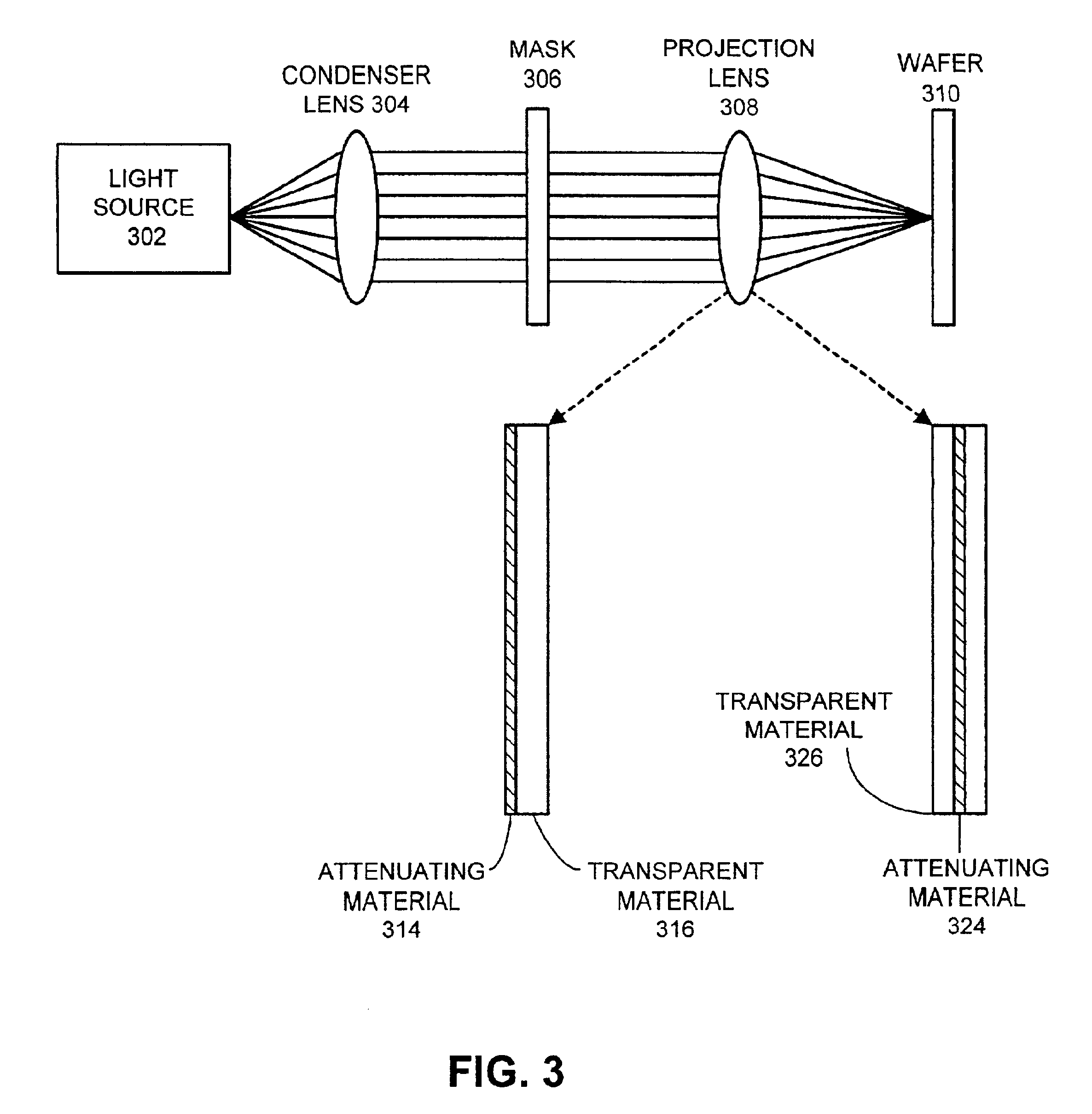
Optical System
FIG. 3 illustrates an optical system including a pupil filter in accordance with an embodiment of the invention. As shown in FIG. 3, radiation emanates from light source 302, which can be any suitable source of radiation such as a laser. This radiation passes through condenser lens 304, and then through mask 306. Mask 306 defines circuit patterns to be projected onto wafer 310. The image of mask 306 passes through projection lens 308, which directs the image onto wafer 310. Wafer 310 is a semiconductor wafer treated with a photoresist layer, or more generally any item to be exposed by the system. During operation, the above-described system transfers the circuitry defined by mask 306 onto wafer 310.
Note that projection lens 308 can include a series of lenses, one or more lenses that perform pupil filtering. As is illustrated in the left-hand example in FIG. 3, a lens that performs pupil filtering can include a transparent material 316 that makes up the lens, such as qu...
PUM
| Property | Measurement | Unit |
|---|---|---|
| optical proximity | aaaaa | aaaaa |
| phase | aaaaa | aaaaa |
| radial distance | aaaaa | aaaaa |
Abstract
Description
Claims
Application Information