

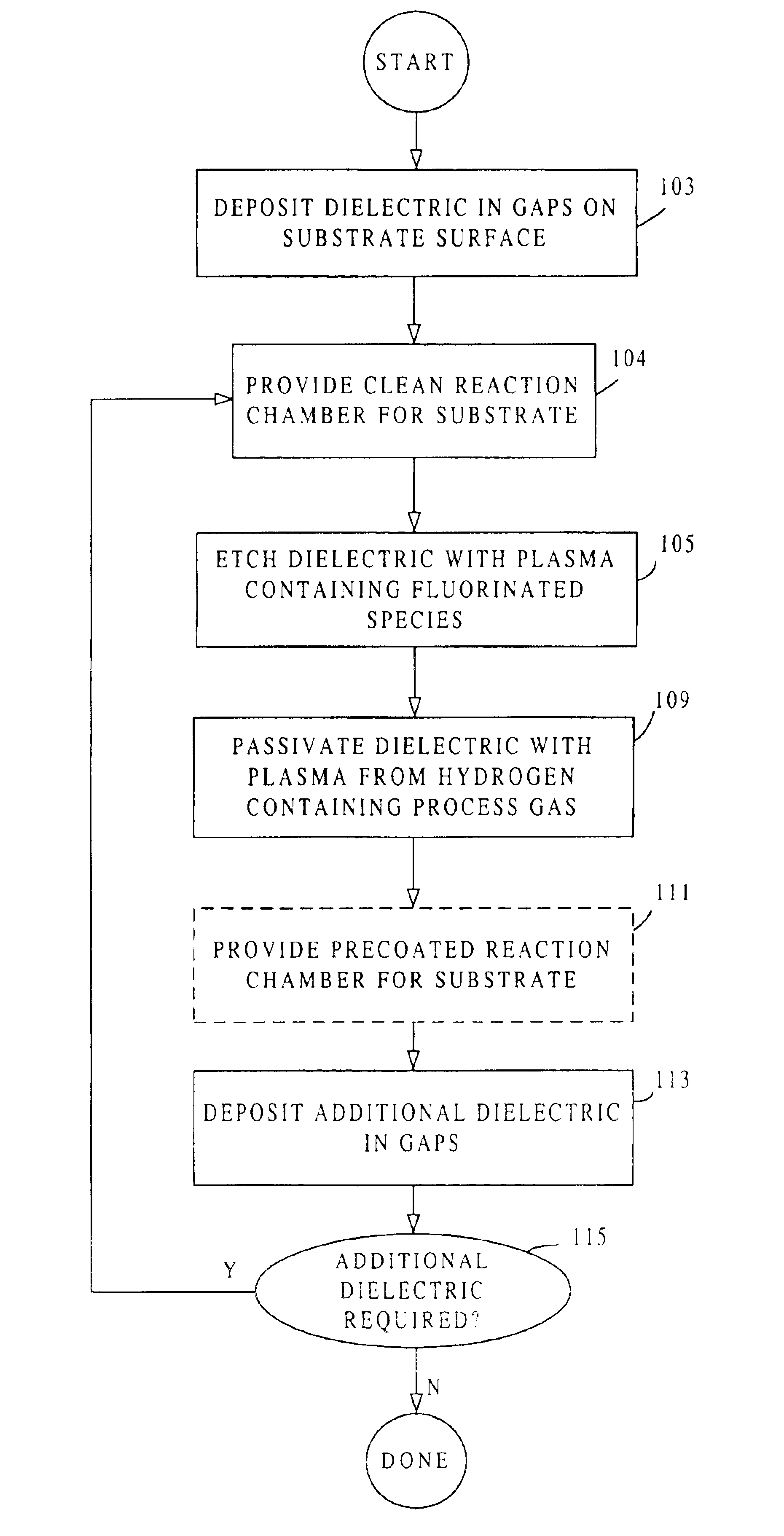
High-density plasma process for filling high aspect ratio structures
a plasma process and high aspect ratio technology, applied in the field of high-density plasma process for filling can solve the problems of voids within the lower portions of gaps, voids in the top part of high aspect ratio structures, and increasing difficulty in void-free filling of high aspect ratio gaps (e.g., ar>3.0:1)
- Summary
- Abstract
- Description
- Claims
- Application Information
AI Technical Summary
Benefits of technology
Problems solved by technology
Method used
Image

Examples
example
FIG. 4 shows fluorine concentration profiles versus dielectric depth for dielectrics deposited by four processes. Importantly, in the one process employing a post-etch hydrogen passivation operation, the maximum concentration of fluorine is reduced by a factor of 3 to 4, from 500-700 ppm to under 200 ppm.
All processes were conducted in a Novellus HDP SPEED reactor. The substrate was flat with unvarying topology.
In the processes identified as 1, 4, and 9, the process conditions were as follows.
DepositionSiH435sccmO265sccmH21000sccmLF2500WattsHF2500WattsEtchNF3150sccmO2300sccmAr90sccmLF1600WattsHFNo bias
In the process identified by the curve labeled H2, the process conditions were as follows:
Deposition and Etch—Same as processes 1, 4, and 9.
PassivationH21500sccmLF4700WattsHFNo bias
The concentration profiles shown in FIG. 4 were obtained by SIMS analysis of deposited dielectric. Interestingly, there are four separate fluorine peaks shown in the profiles. These were caused by four separ...
PUM
| Property | Measurement | Unit |
|---|---|---|
| Temperature | aaaaa | aaaaa |
| Temperature | aaaaa | aaaaa |
| Temperature | aaaaa | aaaaa |
Abstract
Description
Claims
Application Information