
Radiation-hardened transistor fabricated by modified CMOS process

a technology of cmos and transistors, applied in the direction of radiation controlled devices, semiconductor devices, semiconductor/solid-state device details, etc., can solve the problems of ionizing radiation damage, ionizing particle charge release may be trapped in oxide or nitride layers, and circuits become more susceptible to the effects of ionizing radiation

Inactive Publication Date: 2005-01-25
RAYTHEON CO
View PDF4 Cites 28 Cited by
  • Summary
  • Abstract
  • Description
  • Claims
  • Application Information

AI Technical Summary

Benefits of technology

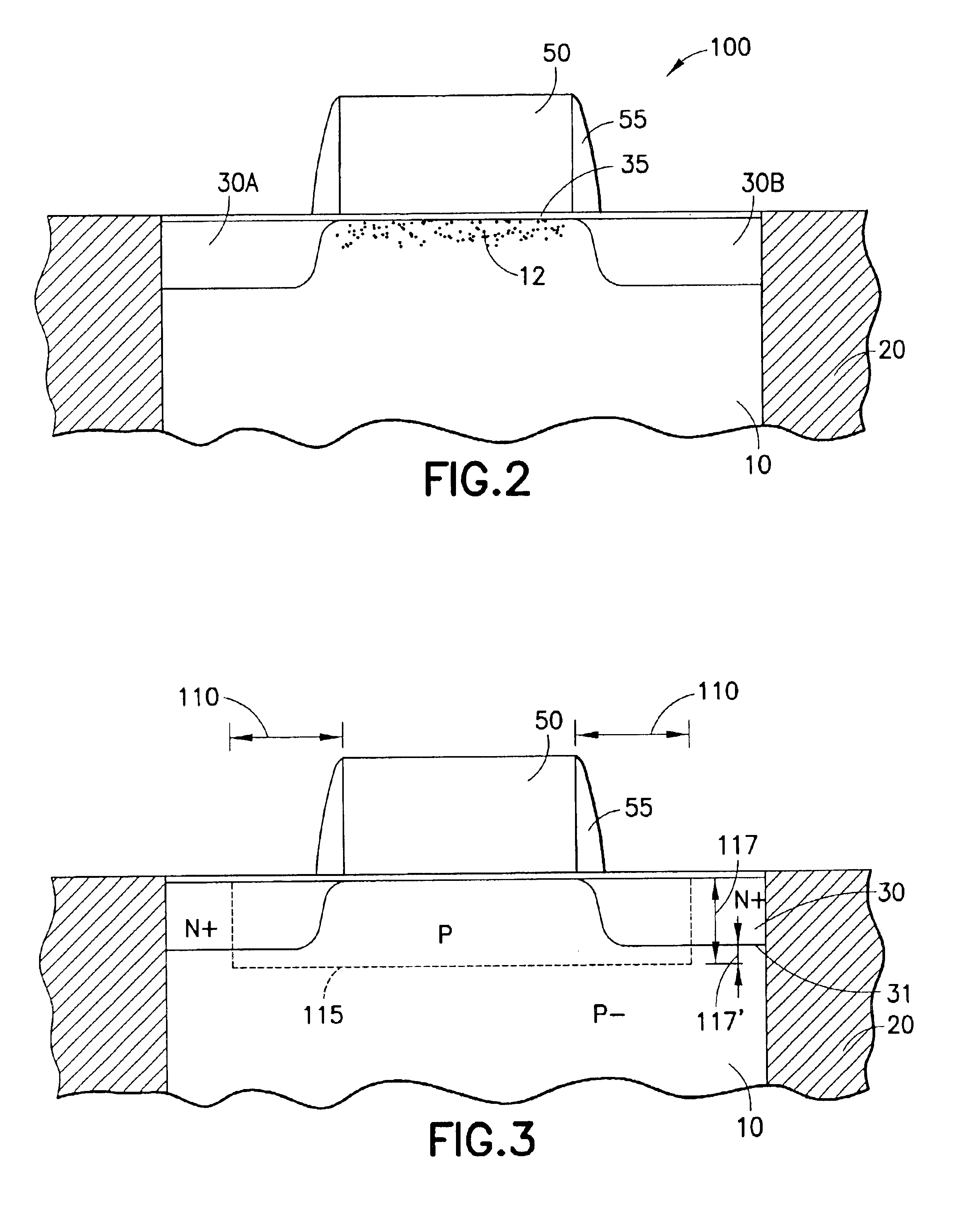
The invention relates to a method of constructing a transistor, such as an NMOS field effect transistor, by adding a step of implanting an area under the gate extending in a first direction between the source and drain, and in a second direction overlapping both the outer edge of the transistor body and an adjacent isolating insulator. The implant may thus be considered to form guard band structures for the transistor that beneficially substantially eliminates the undesirable effects of ionizing radiation. The resulting transistor device is thus radiation hardened, but in a manner that is compatible with conventional IC fabrication line procedures and equipment, and thus in a manner that significantly reduces both cost and complexity.

Problems solved by technology

As transistor and other integrated circuit (IC) dimensions shrink, the circuits become more susceptible to the effects of ionizing radiation.
For example, capacitors in DRAMs may be discharged, cells in SRAMs may change state and other deleterious effects may occur as a result of stray charge and ionizing radiation from radioactive materials or from cosmic rays.
In addition, charge released by an ionizing particle may be trapped in an oxide or nitride layer and increase leakage across a junction, or along a path that nominally blocks charge flow.
For example, charge trapped in the gate oxide of an NMOS transistor may decrease the threshold of the transistor and thus increase the leakage between source and drain in the off state, as well as changing the time during a voltage ramp when it turns on.
The overall effects of radiation-induced damage can result in spurious circuit operation or even in non-functional devices on an integrated circuit.
However, these processes are non-standard and are not readily integrated into a conventional IC fabrication line, and thus their use incurs substantial additional cost and complexity, especially for relatively low volume production runs (e.g., some hundreds or a few thousand ICs).

Method used


Image

  • Radiation-hardened transistor fabricated by modified CMOS process
  • Radiation-hardened transistor fabricated by modified CMOS process
  • Radiation-hardened transistor fabricated by modified CMOS process

Examples


Embodiment Construction

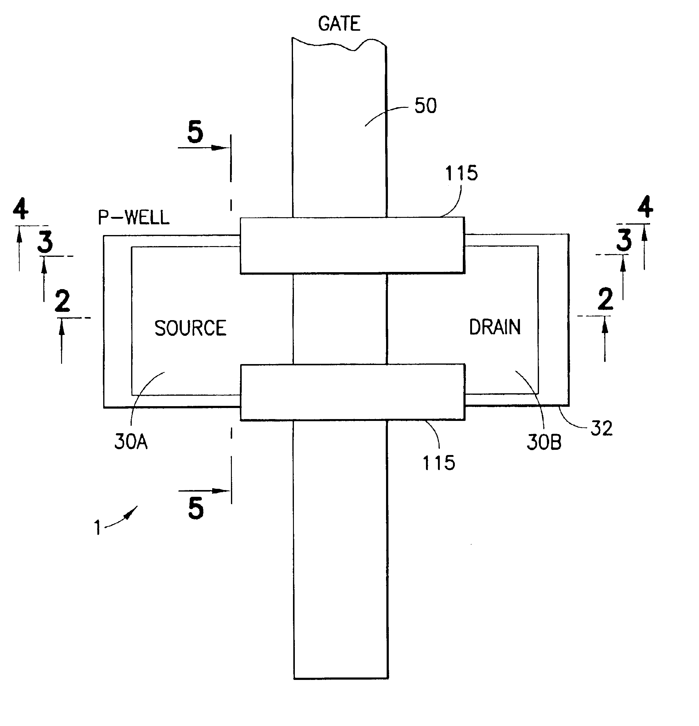
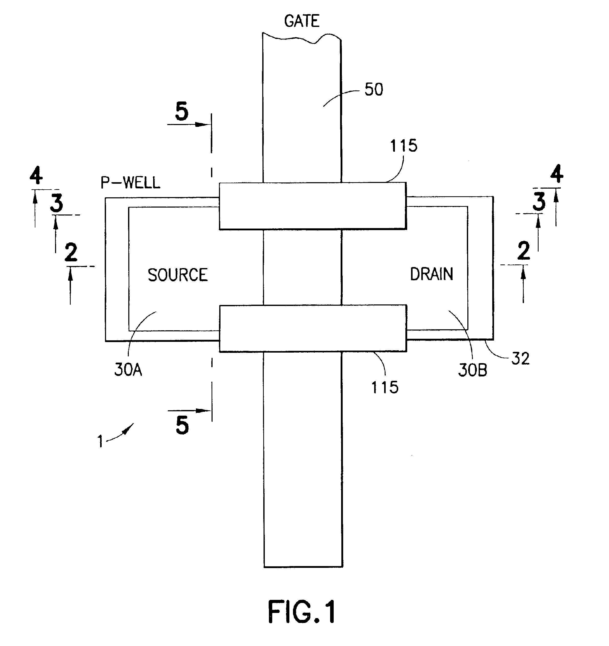
FIG. 1 shows a top view of field effect transistor (FET) 1, such as an NFET, implanted with a radiation-hardening implant forming guard bands 115 according to the invention.

The FET 1 has a source 30A and a drain 30B bisected by a gate 50 that extends past the transistor body in the vertical direction in the drawing. The FET 1 is located in a P-well that can be formed by a conventional method. Two areas of the FET structure, referred to as the guard bands 115, are implanted with a dose of ions to suppress leakage caused by radiation (referred to as a leakage-suppressing dopant and having the same polarity as the FET body). The areas extend along the edges of the transistor body covering the area where the gate 50 crosses the edge of the body and extends into the S / D.

The FET 1 is surrounded by a trench field insulator 20, illustratively CVD oxide deposited in a shallow trench. If space and the thermal budget permit, the insulation could be a thermal oxide also. Having the field insula...


PUM


Abstract

An NMOS field effect transistor (1) is made radiation hard by a pair of guard band implants (115) of limited horizontal extent, extending between the source (30A) and drain (30B) along the edge of the transistor body, and extending only to a limited extent into the field insulator and into the interior of the transistor, leaving an unimplanted area in the center of the body that retains the transistor design threshold voltage.

Description

TECHNICAL FIELDThe field of the invention is radiation-hardened integrated circuits made by a CMOS process.BACKGROUND OF THE INVENTIONAs transistor and other integrated circuit (IC) dimensions shrink, the circuits become more susceptible to the effects of ionizing radiation. For example, capacitors in DRAMs may be discharged, cells in SRAMs may change state and other deleterious effects may occur as a result of stray charge and ionizing radiation from radioactive materials or from cosmic rays.In addition, charge released by an ionizing particle may be trapped in an oxide or nitride layer and increase leakage across a junction, or along a path that nominally blocks charge flow. For example, charge trapped in the gate oxide of an NMOS transistor may decrease the threshold of the transistor and thus increase the leakage between source and drain in the off state, as well as changing the time during a voltage ramp when it turns on. Charge trapped in the field oxide surrounding the device...

Claims


Application Information

Patent Timeline
IPC IPC(8): H01L29/02H01L29/10H01L23/58H01L21/70H01L21/8238
CPCH01L21/823807H01L21/823878H01L23/585H01L29/1041H01L2924/0002H01L2924/00
Inventor LUM, WING Y.
Owner RAYTHEON CO
Learn More