Growth of uniform crystals

a technology of uniform crystals and growth, applied in the direction of crystal growth process, polycrystalline material growth, chemistry apparatus and processes, etc., can solve the problems of non-uniform composition, higher defect density, and above does not provide for forming a uniform alloy crystal, so as to promote uniform crystal growth, uniform crystal growth, and slow melt temperature reduction

Inactive Publication Date: 2005-02-01
AIR FORCE UNITED STATES OF AMERICA AS REPRESENTED BY THE SEC OF
View PDF1 Cites 49 Cited by
  • Summary
  • Abstract
  • Description
  • Claims
  • Application Information

AI Technical Summary

Benefits of technology

Broadly, the present invention provides a method for growing a more uniform crystal by bottom seeding which includes,a) loading a vessel, in its lower portion with a seed crystal,b) adding a charge thereon in said vessel,c) heating the charge to a molten state to form a melt,d) electromagnetically stirring the melt to promote uniformity over the crystal ande) slowly reducing the temperature of the melt over such crystal to grow the latter.

Problems solved by technology

L10-L13, by M. Watanabe et al. which, however, relate to the CZ or top seeding method of crystal growth, with the attendant problems of non-uniform composition and higher defect density due to convection and the steep temperature gradient.
Thus the prior art above does not provide for forming a uniform alloy crystal.

Method used


Image

  • Growth of uniform crystals
  • Growth of uniform crystals
  • Growth of uniform crystals

Examples


Embodiment Construction

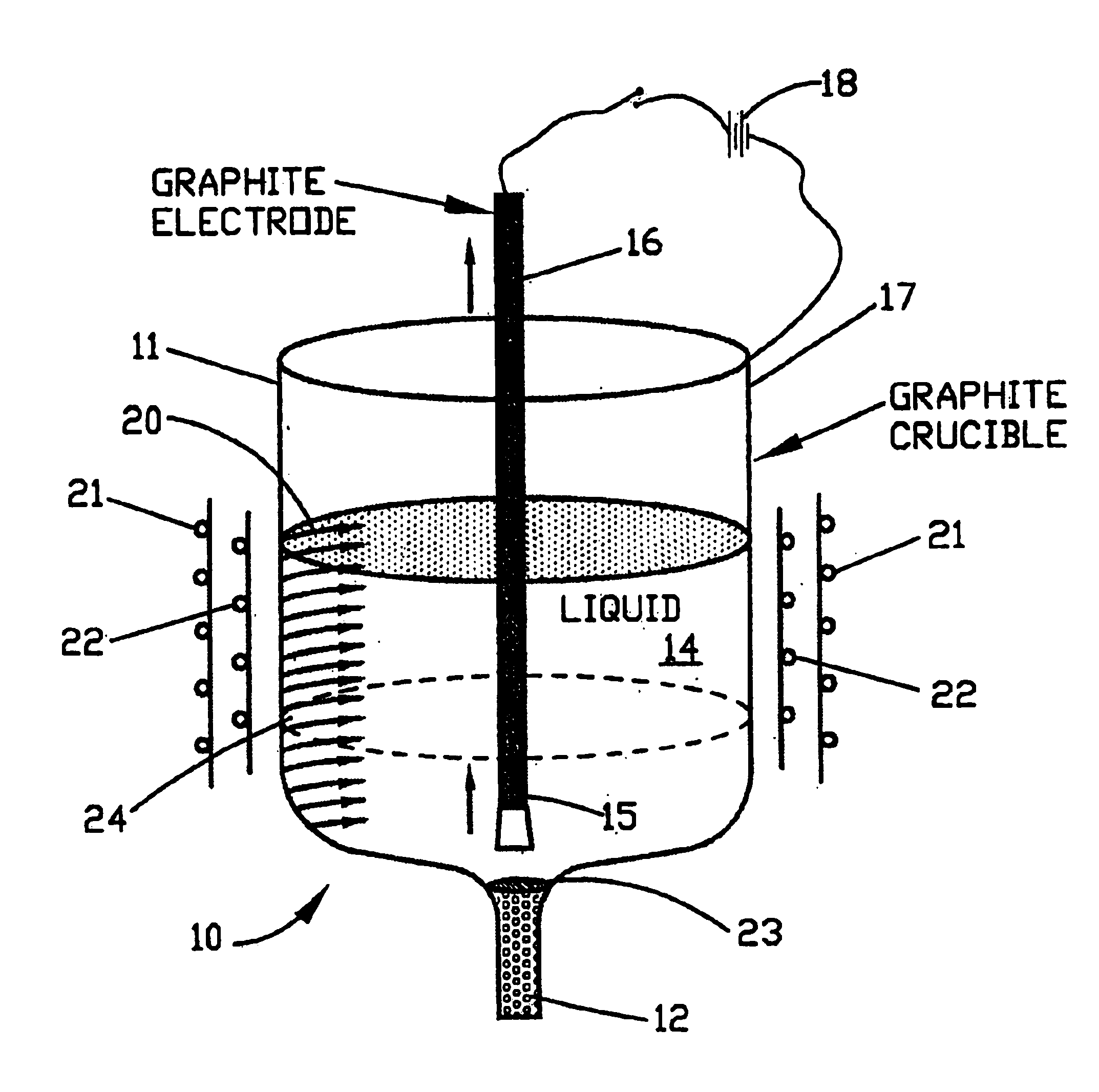
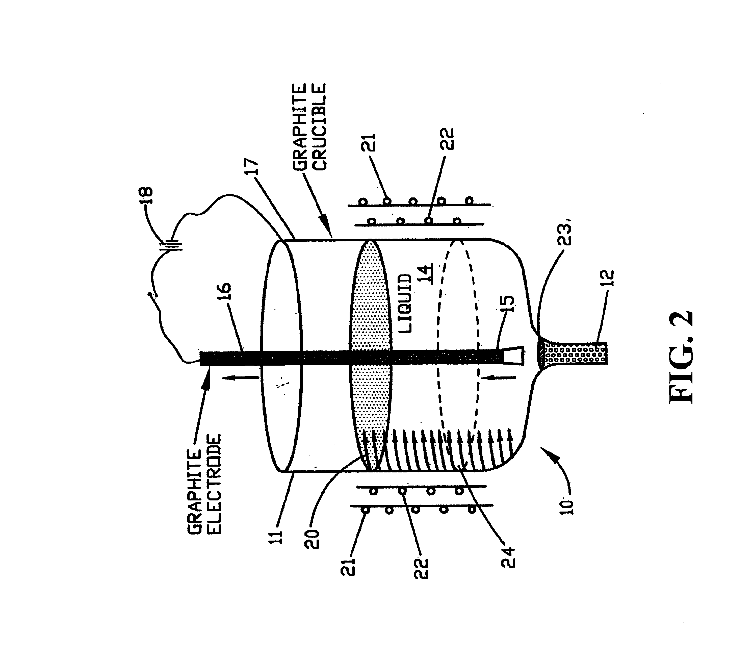
Referring in more detail to the drawings, the present invention utilizes magnetic and electric fields to provide stirring during the growth of semiconductor crystals from bottom-seeded melts. One procedure for growing a crystal with such stirring, is to load a cylindrical crystal growth crucible 11 that is closed at the bottom and open at the top with a single seed crystal 12 at the bottom and a charge of one or more chunks or particles of a solid (at room temperature) on top of it (not shown). The so loaded crucible is then heated by a helical coil 22, so that the temperature increases from bottom to top of the charge, until all of the charge and a small portion of the seed 12, become molten to form melt 14, as indicated in FIG. 2.

A small-diameter electrode 16 made of electrically conducting material that does not chemically react with the molten charge is inserted vertically into the center of the melt so that it extends to a point just above the seed crystal 12 but does not touch...


PUM

PropertyMeasurementUnit
magnetic fieldaaaaaaaaaa
melt heightaaaaaaaaaa
temperatureaaaaaaaaaa

Abstract

The invention provides for growing semiconductor and other crystals by loading a vessel in its lower portion with a seed crystal, loading a charge thereon in the vessel, heating the charge to a molten state and electromagnetically stirring the melt using magnetic and electric fields to obtain a more uniform composition of melt and slowly reducing the temperature of the melt over the crystal to grow a more uniform crystal from such stirred melt.

Description

FIELD OF THE INVENTIONThis invention relates to controlled growth of crystals, particularly for growth of more uniform crystals.BACKGROUND OF THE INVENTIONThe favored research approach to achieve ultra high-quality compound semiconductor crystals is the bottom-seeded method—either the Vertical Gradient Freeze (VGF) or Bridgman technique. There are clear advantages of these methods over the more common top-seeded Czochralski (CZ) method, However, in some cases the crystal growth rate can be severely limited and in others the composition of the crystal can be non-uniform.In the above bottom-seeded method, seed crystal 2 is positioned under growth crystal 4, in turn under melt 6, in vessel 8 as shown in FIG. 1.In the VGF and Bridgman methods of crystal growth (FIG. 1), solidification is initiated either from a seed or from spontaneous nuclei at the bottom of a molten charge as opposed to the CZ method in which a seed is dipped into the melt from the top. Convective stirring due to ther...

Claims


Application Information

Patent Timeline
Patent Type & Authority Patents(United States)
IPC IPC(8): C30B29/10C30B29/40C30B11/00
CPCC30B11/003C30B11/007C30B29/40C30B30/04Y10S117/917Y10T117/10Y10T117/1032
Inventor ISELER, GERALD W.BLISS, DAVID F.TASSEV, VLADIMIR L.
Owner AIR FORCE UNITED STATES OF AMERICA AS REPRESENTED BY THE SEC OF
Why Eureka
Try Eureka