Methods for fabricating an improved floating gate memory cell

a floating gate memory and memory cell technology, applied in the field of semiconductor integrated circuits, can solve the problems of increasing the number of linked transistors and memory cells, reducing the size of flotox transistors, and difficulty in forming an inversion channel between the source and drain of flotox transistors, so as to improve the density of memory cells, improve the size of each memory cell, and improve the effect of floating gate memory cells

Inactive Publication Date: 2005-02-01
MICRON TECH INC
View PDF11 Cites 57 Cited by
  • Summary
  • Abstract
  • Description
  • Claims
  • Application Information

AI Technical Summary

Benefits of technology

The above mentioned problems with non volatile FLOTOX transistors and other problems are addressed by the present invention and will be understood by reading and studying the following specification. A method and structure for an improved floating gate memory cell are provided. The present invention capitalizes on a single step process for defining a shallow trench isolation (STI) region and floating gate that aligns the edges of each with the other. This alignment allows for a significant reduction in the size of each memory cell that correspondingly increases the density of memory cells in a particular area of a memory system. The alignment also facilitates an improved edge profile of the floating gate polysilicon that correspondingly increases data retention due to the elimination of localized tunneling at the field isolation edge. Additionally, the alignment provides for greater erase uniformity by reducing variations due to tunnel oxide thinning at the edge of the field isolation uniformity.
The present invention also employs techniques to increase the area of the top side of the floating gate. The area increase is needed to compensate for the loss in area due to the reduced size of the memory cell that correspondingly reduces the gate coupling ratio (GCR) between the floating gate and the control gate. The techniques include using hemispherical grain (HSG) polysilicon or wings on the top surface of the floating gate. Either HSG polysilicon or wings will increase the surface area of the top side of the floating gate. The increased area maintains or improves the GCR between the floating gate and the control gate of the memory cell, thus, allowing the memory cell to function at reasonable signal levels.

Problems solved by technology

The complexity of these circuits requires the use of an ever increasing number of linked transistors and memory cells.
Storing sufficient charge on the floating gate will make it more difficult to form an inversion channel between the source and drain of the FLOTOX transistor.
One of the present hurdles in reducing the size of the FLOTOX transistor is related to the creation of the floating polysilicon gate and the shallow trench isolation region between adjacent FLOTOX transistors.
Thinning of the tunnel oxide can lead to at least two performance problems.
A first problem is erase uniformity.
A second problem is data retention.
Because of the higher fields and density of charge during erase, in these regions, long term data retention can become a problem.
Another problem arises when the device size is reduced, the gate coupling ratio (GCR) decreases.
If the loss of gate coupling is large enough, this may require the periphery transistors to operatate near their breakdown levels.
The problem with this approach is that the process becomes very complex.

Method used


Image

  • Methods for fabricating an improved floating gate memory cell
  • Methods for fabricating an improved floating gate memory cell
  • Methods for fabricating an improved floating gate memory cell

Examples


Embodiment Construction

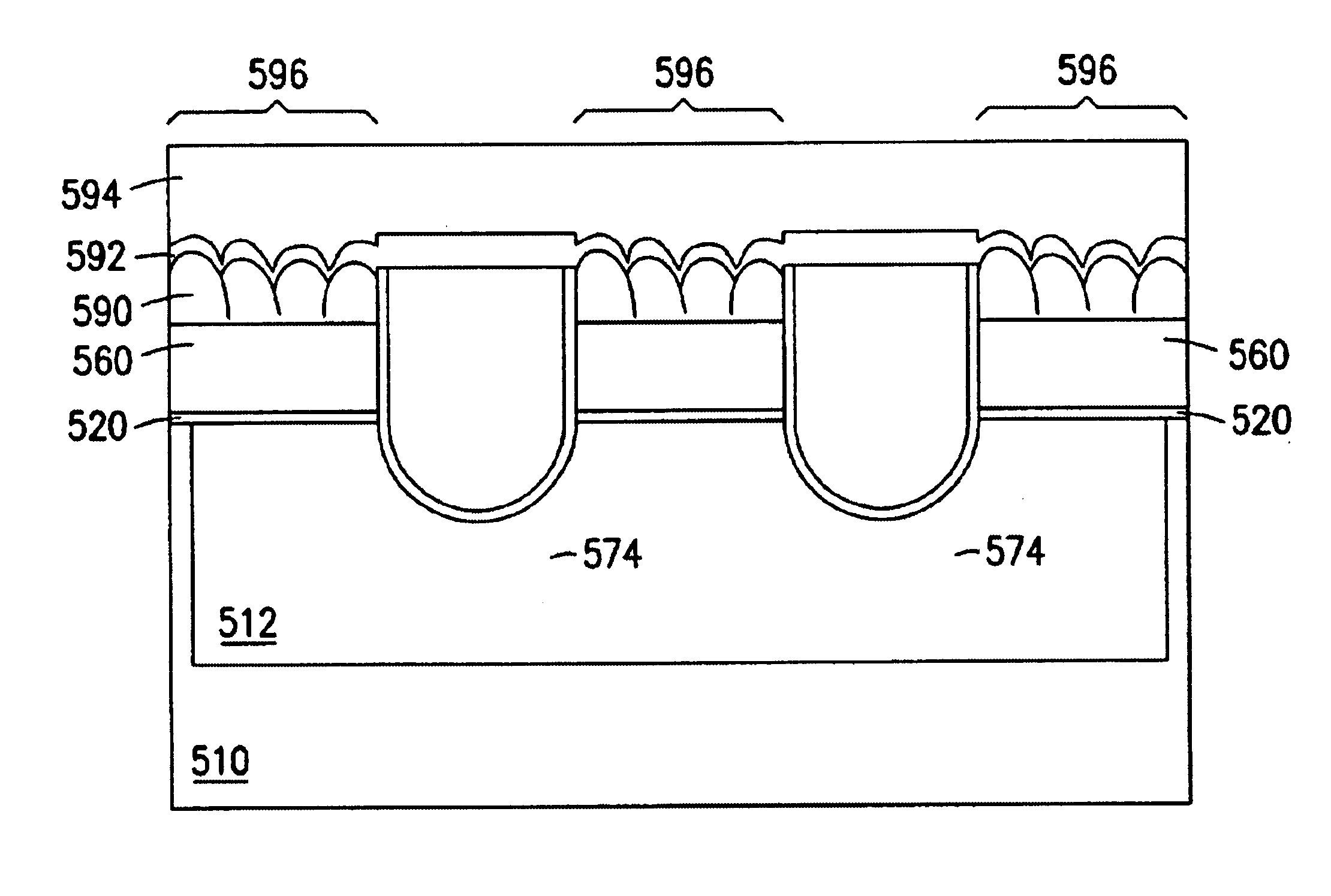
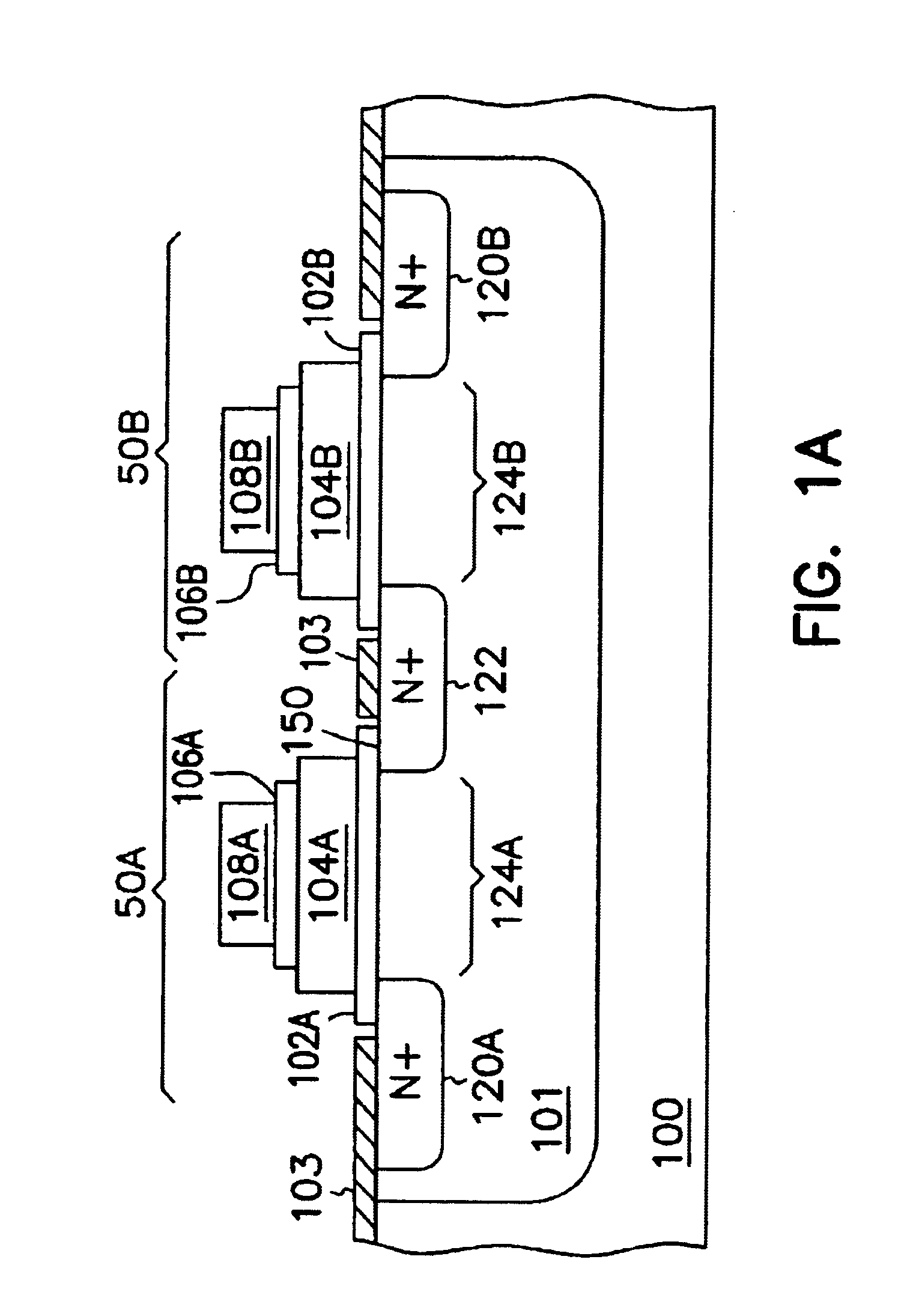
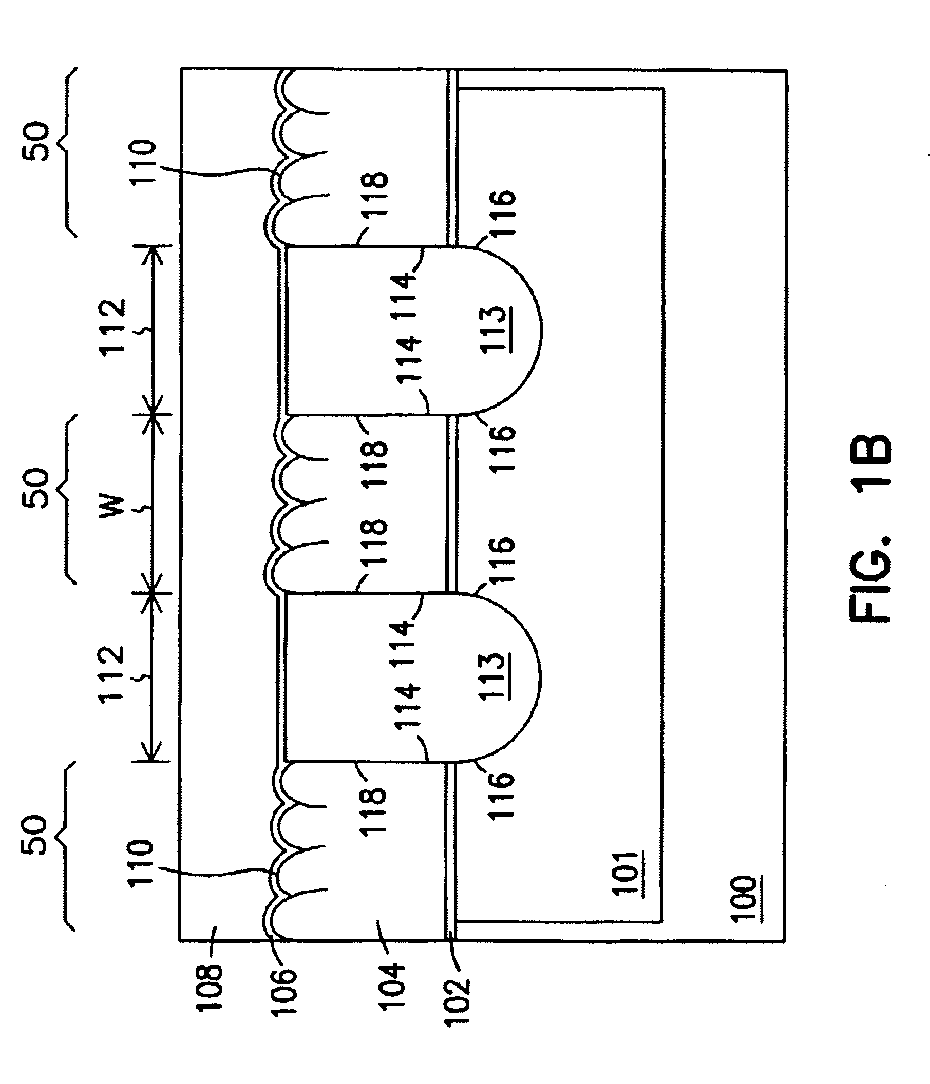
In the following detailed description of the invention, reference is made to the accompanying drawings which form a part hereof, and in which is shown, by way of illustration, specific embodiments in which the invention may be practiced. In the drawings, like numerals describe substantially similar components throughout the several views. These embodiments are described in sufficient detail to enable those skilled in the art to practice the invention. Other embodiments may be utilized and structural, logical, and electrical changes may be made without departing from the scope of the present invention.

The terms wafer and substrate used in the following description include any structure having an exposed surface with which to form the integrated circuit (IC) structure of the invention. The term substrate is understood to include semiconductor wafers. The term substrate is also used to refer to semiconductor structures during processing, and may include other layers that have been fabr...


PUM


Abstract

Methods for fabricating improved floating gate memory cells are provided. A substrate and a first insulating layer are fabricated, where the first insulating layer is formed on the substrate. A shallow trench isolation (STI) region is fabricated having walls that form edges in the substrate and edges to a first conducting layer where the edges of the first conducting layer are aligned with the edges of the substrate. A second insulating layer is formed on the first conducting layer and a second conducting layer formed on the first insulating layer. The invention also includes a method that capitalizes on a single step process for defining the STI region and the floating gate for a memory cell that aligns edges formed in the substrate by the walls of the STI region with the edges of the floating gate formed by the walls of the STI region.

Description

FIELD OF THE INVENTIONThe present invention relates generally to semiconductor integrated circuits. More particularly, it pertains to a method and structure for an improved floating gate memory cell.BACKGROUND OF THE INVENTIONModern integrated circuit technology relies on transistors and memory cells to formulate vast arrays of functional circuits. The complexity of these circuits requires the use of an ever increasing number of linked transistors and memory cells. As the number of transistors and memory cells required increases, the surface area that can be dedicated to a single component dwindles. Today, also, high reliability is needed in each component to reduce the amount of redundancy needed to guarantee proper operation. Additionally, it is desired to have uniformity among memory cells to facilitate uniform erasure and avoid charge leakage for such memory devices. Thus, it is desirable to construct integrated circuit components which have higher reliability and greater unifor...

Claims


Application Information

Patent Timeline
Patent Type & Authority Patents(United States)
IPC IPC(8): H01L29/423H01L27/115H01L29/40H01L21/70H01L21/8247
CPCH01L27/115H01L29/42324H01L27/11521H10B69/00H10B41/30
Inventor RUDECK, PAUL J.
Owner MICRON TECH INC
Why Eureka
Try Eureka