Exposure apparatus, substrate processing system, and device manufacturing method

a technology of substrate processing and equipment, applied in the direction of photomechanical equipment, instruments, printing, etc., can solve the problems of narrowing the depth of focus, unable to meet the recent tight requirements by conventional methods referred to above or by similar methods, and the numerical aperture of the projection optical system cannot be increased too much, so as to achieve the effect of improving the productivity of the devices serving as end products, high yield and high integration microdevices

Inactive Publication Date: 2005-02-08
NIKON CORP
View PDF9 Cites 103 Cited by
  • Summary
  • Abstract
  • Description
  • Claims
  • Application Information

AI Technical Summary

Benefits of technology

The present invention was made under the circumstances above, and has as its object to provide an exposure apparatus and a substrate processing system that contributes to improving the productivity of devices, which are end products.
In addition, in a lithographic process, by performing exposure using any one of the first to fourth exposure apparatus in the present invention, a pattern can be formed accurately on a substrate, which allows high integration microdevices to be produced with high yield. Accordingly, in the present invention, furthermore from another aspect, there is provided a device manufacturing method using any one of the first to fourth exposure apparatus in the present invention.

Problems solved by technology

It is, however, becoming difficult to achieve the recent tight requirements by the conventional methods referred to above or by similar methods.
That is, the numerical aperture of the projection optical system cannot be increased too much, since it leads to narrowing the depth of focus.
However, new problems have occurred with such wavelength or light having a shorter wavelength; that they are greatly absorbed by air (oxygen), water vapor, hydrogen carbonate gas, or the like.
In addition, increasing the speed of the wafer stage or the reticle stage may cause the throughput or exposure accuracy to reduce.
That is, increasing the speed of these stages leads to an increase in settling time for position setting, or an increase in synchronous settling time of both stages on scanning exposure.
In addition, increasing the speed also increases vibration, which may aggravate the positional controllability of the stages.
With the double wafer stage type exposure apparatus, however, the reaction force caused by the movement of the wafer stage where operations such as alignment is performed may be the cause of vibration in the other wafer stage where exposure is performed.
This may lead to a decrease in exposure accuracy, which may reduce the yield of the end products, or the devices.
Accordingly, from an overall perspective, productivity of the devices may not always be improved.
In addition, even if the double wafer stage method is employed, the problem of the transmittance of the exposure light decreasing due to absorption of the exposure light referred to earlier still remains.
Also, if the double wafer stages are simply employed, the footprint will increase due to larger stage supporting beds.
Since the running cost of a clean room is extremely expensive, as a whole, the productivity of the devices may not always be improved.

Method used


Image

  • Exposure apparatus, substrate processing system, and device manufacturing method
  • Exposure apparatus, substrate processing system, and device manufacturing method
  • Exposure apparatus, substrate processing system, and device manufacturing method

Examples


first embodiment

<<First Embodiment>>

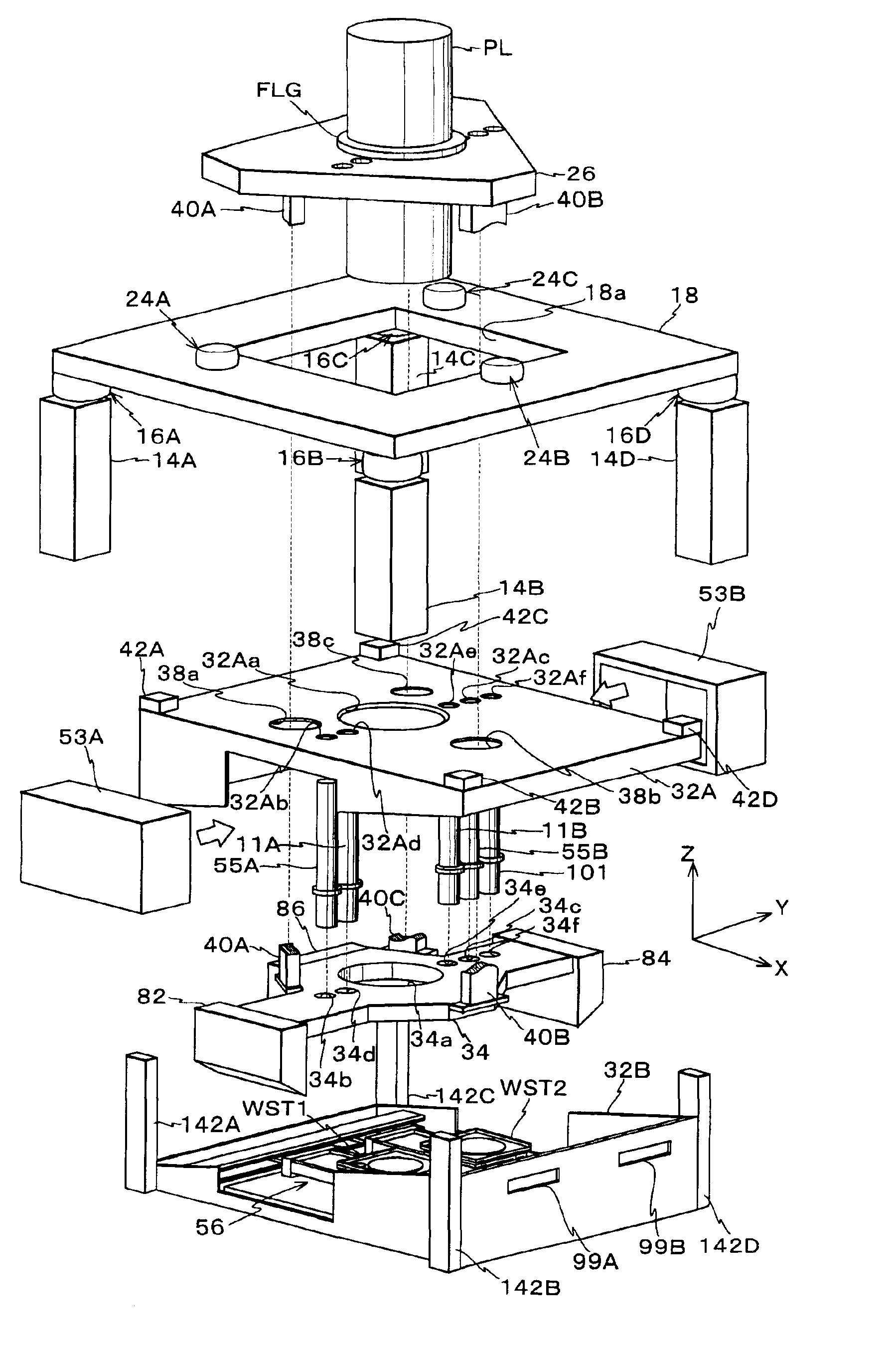
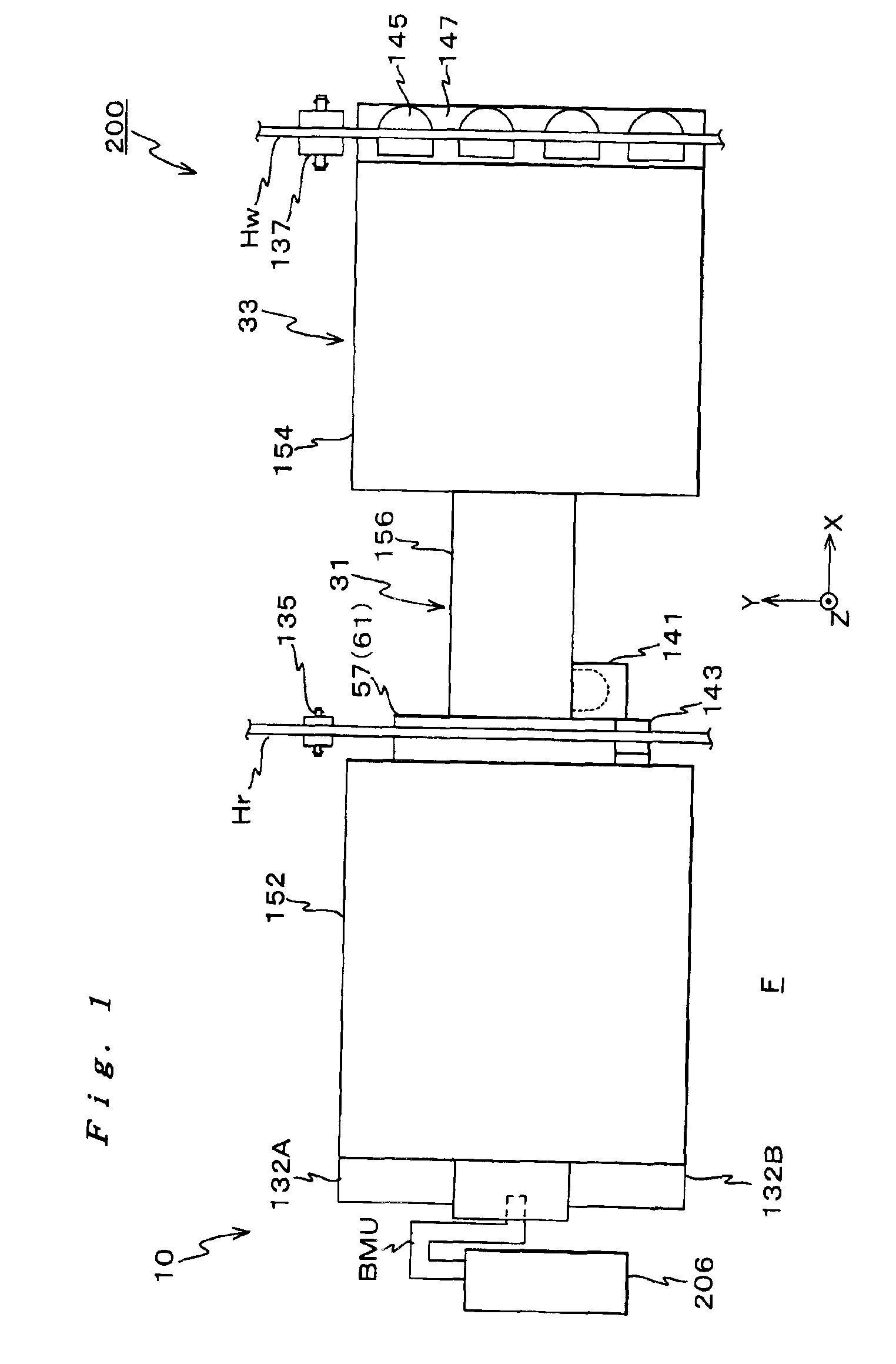
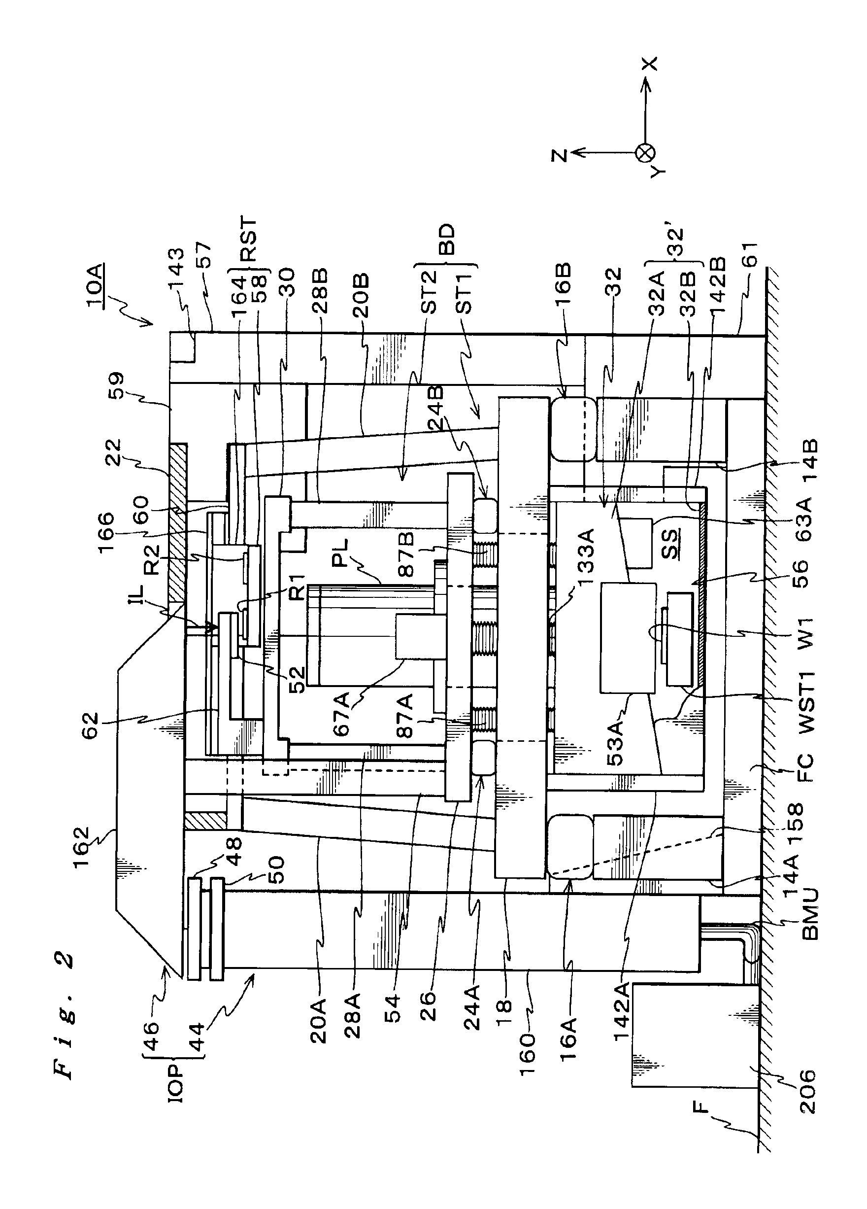
Following is a description of a first embodiment related to the present invention, referring to FIGS. 1 to 16. FIG. 1 shows a planar view of an entire substrate processing system related to the first embodiment including an exposure apparatus related to the present invention.

A substrate processing system 200 shown in FIG. 1 is arranged in a clean room where the level of cleanliness is around class 100 to 1000. The substrate processing system 200 comprises: an exposure apparatus 10; a coater developer (hereinafter referred to as “C / D”) 33 serving as a substrate processor; and an interface section 31 which connects exposure apparatus 10 and C / D 33 inline, arranged on a floor surface F of the clean room in an X-axis direction (the lateral direction on the page surface of FIG. 1) at a predetermined interval.

Inside exposure apparatus 10, it comprises: a main body chamber 152 serving as a total chamber that houses an exposure apparatus main body (to be descri...

second embodiment

<<Second Embodiment>>

Next, a second embodiment of the present invention is described, referring to FIGS. 17A and 18. Structures and components identical or equivalent to those described in the first embodiment are designated with the same reference numerals, and the description thereabout is briefly made or is entirely omitted.

In the second embodiment, instead of seal mechanism 85 provided on the lower end of the projection optical system PL in the first embodiment described earlier, a seal mechanism 85′ as is shown in FIG. 17A is provided as a seal mechanism. Other portions are identical with the first embodiment.

In seal mechanism 85′, a stop ring 79, which supports a first lens 77 (closest to the image plane) serving as a lens from below at three points at an angle of around 120 degrees close to its circumference portion, is connected to projected portions 21A, 21B, and 21C (projected portion 21C arranged in the depth of the page surface is not shown) provided on the low...

third embodiment

<<Third Embodiment>>

Next, a third embodiment of the present invention is described, referring to FIG. 17B. Structures and components identical or equivalent to those described in the above first and second embodiments are designated with the same reference numerals, and the description thereabout is briefly made or is entirely omitted.

In the third embodiment, instead of seal mechanism 85 provided on the lower end of the projection optical system PL in the first embodiment described earlier, a seal mechanism 85″ as is shown in FIG. 17B is provided as a seal mechanism. Other portions are identical with the first embodiment.

In seal mechanism 85″, as in the description so far, a first lens 77 (closest to the image plane) is arranged under projection optical system PL. And similar to seal mechanism 85′, the first lens 77 is supported from below by a stop ring 79 connected to projected portions 21A, 21B, and 21C (projected portion 21C arranged in the depth of the page surface is...


PUM

PropertyMeasurementUnit
wavelengthaaaaaaaaaa

Abstract

A first main body unit for supporting a substrate stage is supported at four points by vibration isolators, and a second main body unit is supported on the first main body unit at three points by second vibration isolators. This allows the first main body unit and the substrate stage to be supported stably with high rigidity, and for example, allows maintenance on the stage portion from the back side of the apparatus, which is not possible with the first main body unit supported at three points. Further, the apparatus comprises vibration isolation units connected in series in two platforms, which has a great effect of suppressing background vibration from the floor surface. Accordingly, exposure with high precision can be performed which improves the yield of devices, and the reduced maintenance time can improve the operation rate, consequently leading to an improvement in productivity of devices as end products.

Description

BACKGROUND OF THE INVENTION1. Field of the InventionThe present invention relates to exposure apparatus, substrate processing systems, and device manufacturing methods, and more particularly to an exposure apparatus used in a lithographic process when manufacturing devices such as a semiconductor device, a liquid crystal display device, a plasma display device, or a thin film magnetic head, a substrate processing system having the exposure apparatus and a substrate processor connected inline to the exposure apparatus, and a device manufacturing method using the exposure apparatus.2. Description of the Related ArtIn conventional lithographic process for manufacturing devices such as semiconductors, various exposure apparatus have been used. In recent years, the ones mainly used are projection exposure apparatus that move in a step-by-step fashion, such as a reduction projection exposure apparatus based on a step-and-repeat method, that is, the so-called stepper, or a scanning project...

Claims


Application Information

Patent Timeline
Patent Type & Authority Patents(United States)
IPC IPC(8): G03F7/20H01L21/027
CPCG03F7/70766G03F7/709G03F7/70833H01L21/027
Inventor NISHI, KENJI
Owner NIKON CORP
Why Eureka
Try Eureka