Thin film transistor, fabrication method thereof and liquid crystal display having the thin film transistor

a fabrication method and thin film technology, applied in the direction of identification means, instruments, optics, etc., can solve the problems of reducing the electrical characteristic or long-term reliability, the picture quality is affected, so as to improve the fabrication yield and suppress the parasitic capacitance

Inactive Publication Date: 2005-02-15
UNIFIED INNOVATIVE TECH
View PDF18 Cites 101 Cited by
  • Summary
  • Abstract
  • Description
  • Claims
  • Application Information

AI Technical Summary

Benefits of technology

An object of the present invention is to provide a thin film transistor which is a bottom-gate-type thin film transistor in which a channel protection film is formed, suppresses the parasitic capacitances, and improves the fabrication yield, and to provide a fabrication method thereof and a liquid crystal display having the thin film transistor.

Problems solved by technology

An active matrix type liquid crystal display using this thin film transistor as a switching element has a problem in which a pixel effective voltage is reduced due to a field-through voltage resulted from the parasitic capacitances Cp, thereby generating a degradation of picture quality such as flickering of the display, a reduction in contrast and the like.
Therefore, permanent damages such as a trap level in a film and the like due to ion bombardment are generated to an SiNx film of the channel protection film 110, and a possibility of a reduction in electric characteristics or a long-term reliability of the thin film transistor exists, thereby resulting in an obstacle for improving a fabrication yield.

Method used


Image

  • Thin film transistor, fabrication method thereof and liquid crystal display having the thin film transistor
  • Thin film transistor, fabrication method thereof and liquid crystal display having the thin film transistor
  • Thin film transistor, fabrication method thereof and liquid crystal display having the thin film transistor

Examples


example 1

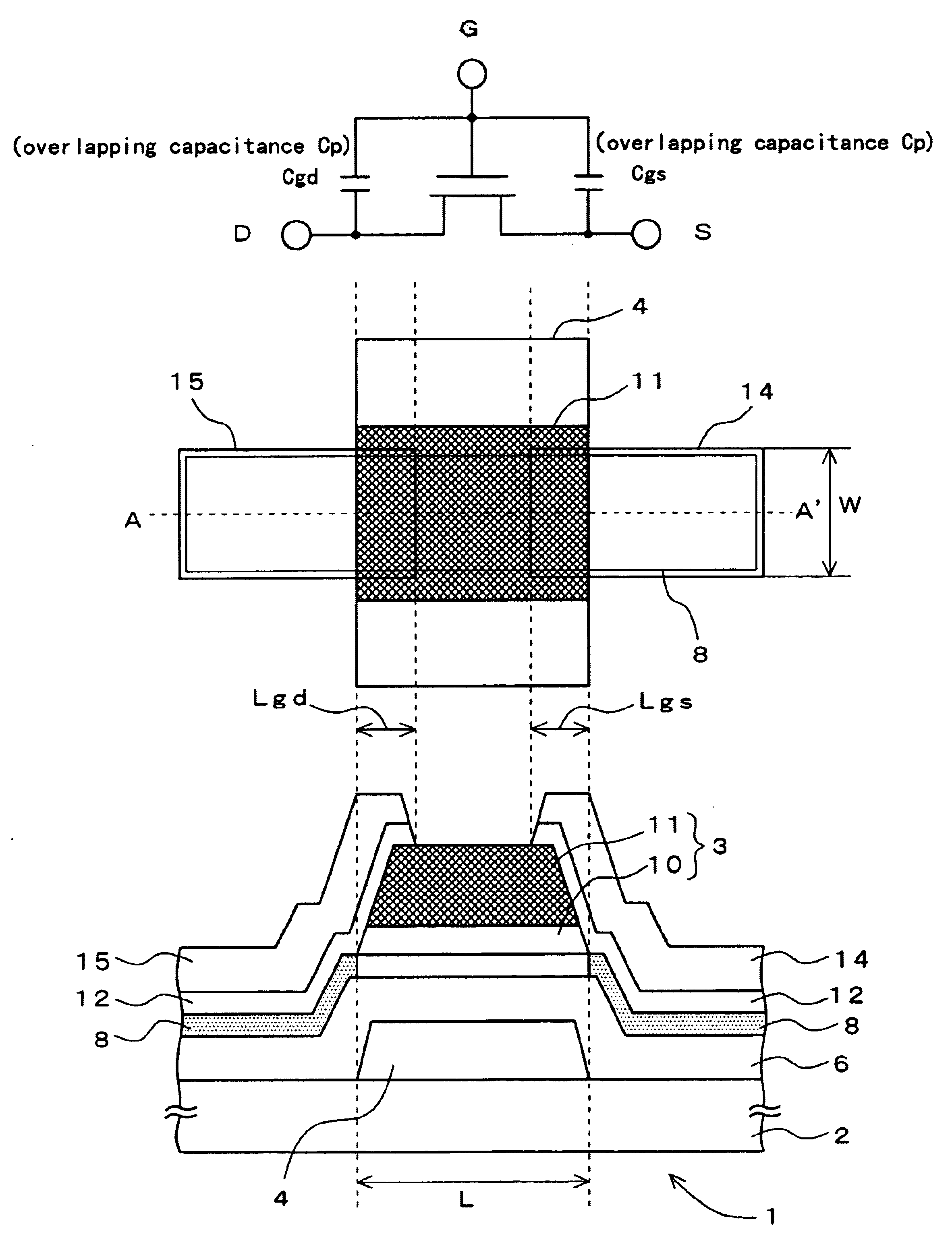
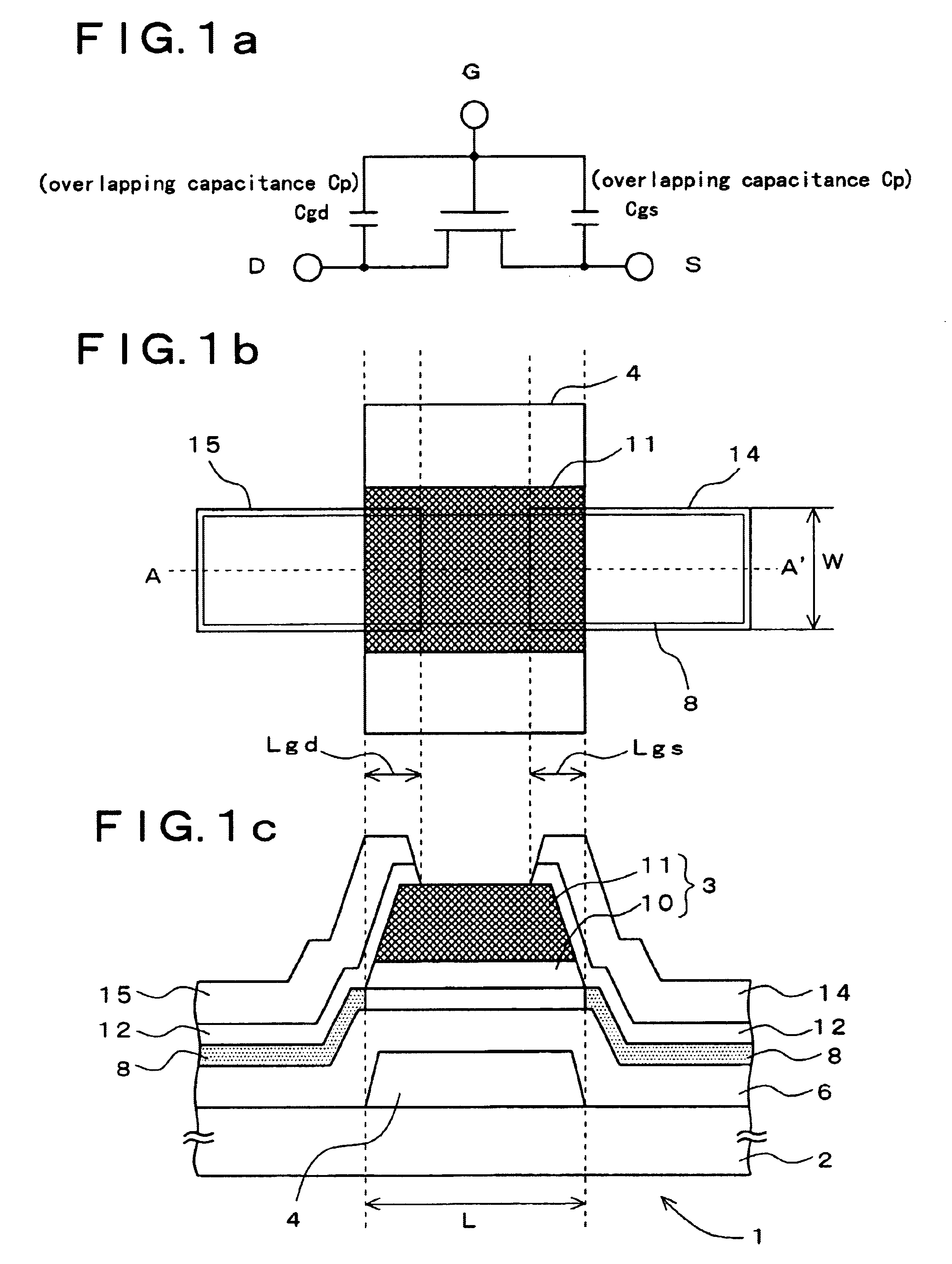
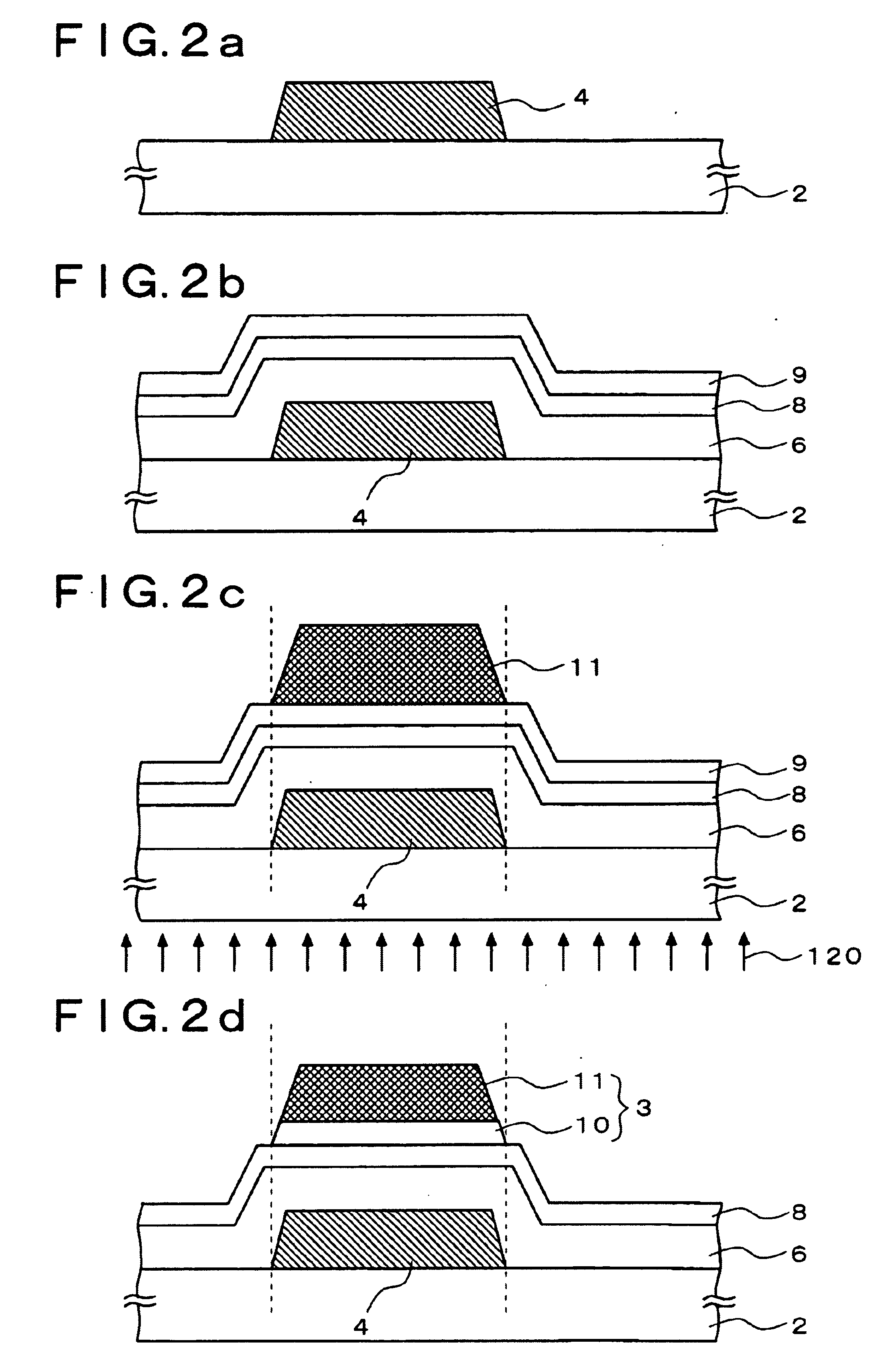
Example 1 is an example of applying this embodiment to a thin film transistor in which a-Si is used for an operational semiconductor film. First, a fabrication process of this thin film transistor is described with reference to FIG. 2a through FIG. 4b.

As shown in FIG. 2a, a glass substrate 2 of, for example, Corning Corporation #1737 is used as an insulative substrate. A chrome (Cr) thin film is deposited from 100 to 300 nm in film thickness, preferably to 150 nm on the glass substrate 2 by sputtering. It will be noted that tantalum (Ta), molybdenum (Mo), aluminum (Al) alloy and the like can also be used in place of Cr. Next, a resist is coated on a whole surface by the usual photolithography process, patterned, and then the Cr thin film is etched by a wet etching with the use of a resist pattern as a mask to form the gate electrode 4.

Then, as shown in FIG. 2b, the gate insulating film 6 is formed by depositing, for example, an SiNx film from 200 to 500 nm in thickness, preferably ...

example 2

Example 2 is an example applying this embodiment to a low-temperature polysilicon thin film transistor (p-SiTFT) having an LDD (light doping drain) structure. Degradation of TFT characteristics due to a hot carrier injection can be prevented by providing an LDD area having a high resistance between a channel and a source and drain area having a low resistance.

First, the fabrication process of this thin film transistor is described with reference to FIG. 9a through FIG. 12b. As shown in FIG. 9a, for example, the glass substrate 2 by Coming Corporation #1737 is used as the insulative substrate. A Cr thin film is deposited on the glass substrate 2 by sputtering until the film thickness is equal to 100 to 300 nm, preferably equal to 150 nm. It will be noted that Ta, Mo, Al alloy or the like can also be used instead of Cr. Next, the gate electrode 4 is formed by coating the resist on a whole surface by the usual photolithography process, patterning the resist, etching the Cr thin film by...

example 3

Example 3 is an example applying this embodiment to a CMOS-type thin film polysilicon transistor (p-SiTFT) and a liquid crystal display having an integrated peripheral circuit which uses the CMOS-type thin film polysilicon transistor (p-SiTFT). First, a fabrication process of this thin film transistor is described with reference to FIG. 14a through FIG. 16c.

As shown in FIG. 14a, a glass substrate 2 by for example Corning Corporation #1737 is used as the insulative substrate. A Cr thin film is deposited on the glass substrate 2 by sputtering until the film thickness is equal to 100 to 300 nm, preferably equal to 150 nm. It will be noted that Ta, Mo, Al alloy or the like can also be used instead of Cr. Next, the gate electrodes 4 and 5 are formed by coating the resist on a whole surface by the usual photolithography process, patterning the resist, etching the Cr thin film by the wet-etching using the resist pattern as a mask. Then, using the PECVD method, for example, an SiNx film is...


PUM

PropertyMeasurementUnit
thicknessaaaaaaaaaa
thicknessaaaaaaaaaa
thicknessaaaaaaaaaa

Abstract

The present invention relates to a thin film transistor, a fabrication method thereof and a liquid crystal display having the thin film transistor, and an object of the present invention is to provide a thin film transistor which improves a fabrication yield, a fabrication method thereof and a liquid crystal display having the thin film transistor. In a bottom-gate-type thin film transistor 1 having a gate electrode 4 formed on a substrate, a gate insulating film 6 formed on the gate electrode, an operational semiconductor film 8 formed on the gate insulating film 6 on the gate electrode 4, a channel protection film 3 formed on the operational semiconductor film, and a source and a drain electrodes 14 and 15 formed on both sides of the top surface of the channel protection film 3 connected to the operational semiconductor film with the operational semiconductor, and the channel protection film 3 has a first insulating layer 10 contacting to an upper interface of the operational semiconductor film 8 and a second insulating layer 11 formed on the first insulating layer.

Description

BACKGROUND OF THE INVENTION1. Field of the InventionThe present invention relates to a thin film transistor, a fabrication method thereof and a liquid crystal display having the thin film transistor.2. Description of the Related ArtOne of the switching elements used in an active matrix type liquid crystal display is a thin film transistor (TFT). A structure of the thin film transistor is divided roughly into the so-called bottom-gate-type inverted staggered structure in which a gate electrode is formed on a glass substrate side rather than source and drain electrodes side and the so-called top-gate-type staggered structure or planer-type structure in which the source and the drain electrodes are formed on a glass substrate side rather than a gate electrode. Among these, a bottom-gate-type thin film transistor can be further divided into two structures. One is a structure in which a channel protection film is formed on an operational semiconductor film forming a channel portion and t...

Claims


Application Information

Patent Timeline
Patent Type & Authority Patents(United States)
IPC IPC(8): H01L21/70H01L21/02H01L29/786H01L29/66H01L21/336H01L27/12H01L21/84G09F9/30G02F1/136G02F1/1368H01L21/77
CPCH01L27/1214H01L29/78621H01L29/66765G02F1/136
Inventor ZHANG, HONG YONG
Owner UNIFIED INNOVATIVE TECH
Why Eureka
Try Eureka