Method for manufacturing semiconductor integrated circuit
- Summary
- Abstract
- Description
- Claims
- Application Information
AI Technical Summary
Benefits of technology
Problems solved by technology
Method used
Image

Examples
first embodiment
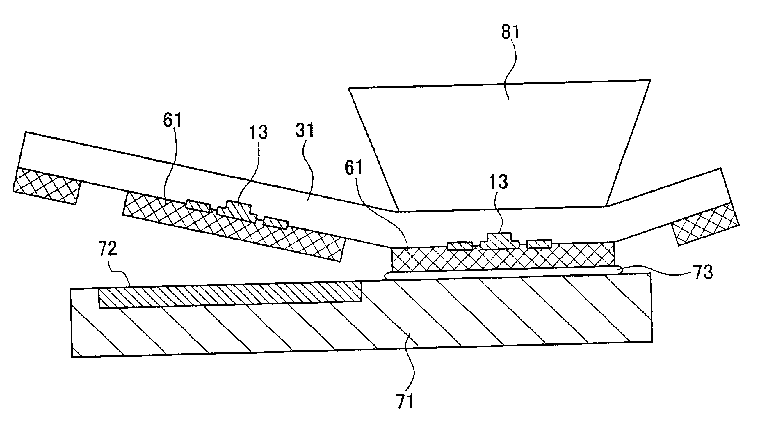
First Step:
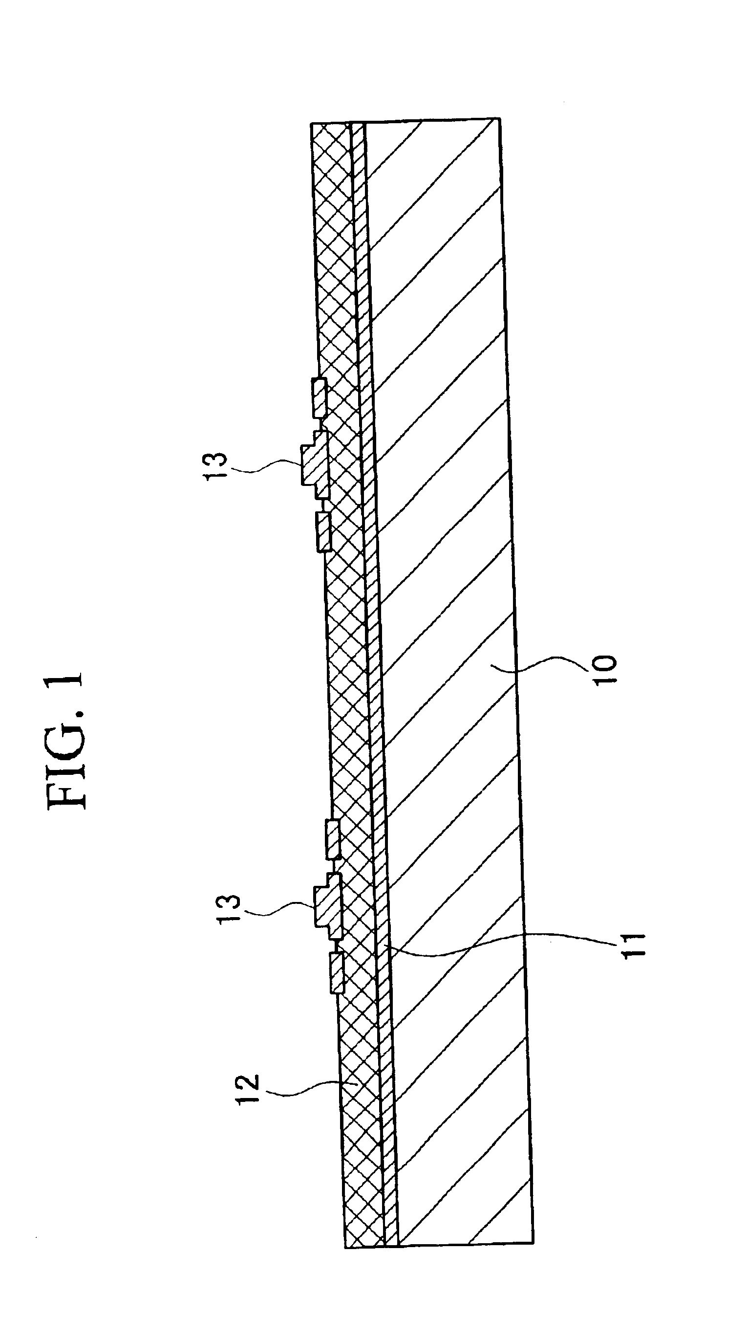
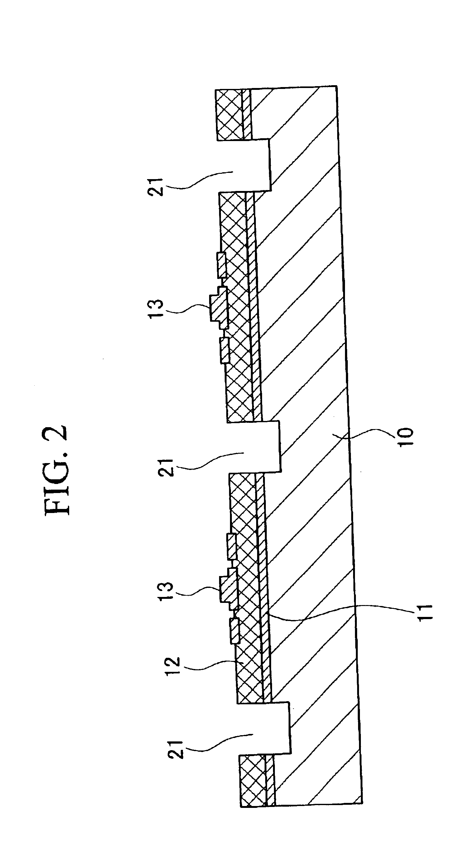
FIG. 1 is a diagram showing a schematic cross-sectional view for explaining the first step of a method for manufacturing a semiconductor integrated circuit according to the embodiment of the present invention. In FIG. 1, a substrate 10 is a semiconductor substrate, and in this embodiment, the substrate 10 is a GaAs compound semiconductor substrate. A sacrificial layer 11 is disposed as the lowest layer in the substrate 10. The sacrificial layer 11 is made of aluminum-arsenic (AlAs) and has a thickness of about several hundred nm, for example.
A functional layer 12 may be disposed on the sacrificial layer 11. The thickness of the functional layer 12 is, for instance, between about 1 to 20 μm. A semiconductor device (semiconductor element) 13 is formed on the functional layer 12. Examples of the semiconductor device 13 include, for instance, a light emitting diode (LED), a vertical cavity surface emitting laserdiode (VCSEL), a photodiode (PD), a high electron mobility transi...
second embodiment
Next, in the second embodiment of the present invention, the case in which a silicon transistor (a silicon semiconductor element) is attached to a glass substrate for liquid crystal will be explained. The first to eleventh steps of the second embodiment correspond to the first to eleventh steps of the first embodiment. The significant difference between the first and second embodiments is that the method used for selectively etching the sacrificial layer in the fourth step is different.
In the first step of the second embodiment, a silicon transistor is formed on a silicon-on-insulator (SOI) substrate using an ordinary process. Here, it is possible to form an integrated circuit which is a silicon device, a photodiode, a transistor, or a diode instead of the silicon transistor. A silicon oxide membrane which becomes a sacrificial layer is provided with the SOI substrate.
In the second step, separation grooves are formed on the SOI substrate. Each separation groove has a depth deep enou...
PUM
 Abstract
Description
Claims
Application Information
 - Generate Ideas
- Intellectual Property
- Life Sciences
- Materials
- Tech Scout
- Unparalleled Data Quality
- Higher Quality Content
- 60% Fewer Hallucinations
Browse by: Latest US Patents, China's latest patents, Technical Efficacy Thesaurus, Application Domain, Technology Topic, Popular Technical Reports.
© 2025 PatSnap. All rights reserved.Legal|Privacy policy|Modern Slavery Act Transparency Statement|Sitemap|About US| Contact US: help@patsnap.com