Apparatus and method of compensating for phase delay in semiconductor device

a semiconductor device and phase delay technology, applied in the field of semiconductor devices, can solve problems such as rlc mismatch, power supply voltage vddq or ground voltage vssq may be shaken, and performance degradation, and achieve the effect of preventing the occurrence of skew

Active Publication Date: 2005-02-22
CONVERSANT INTPROP MANAGEMENT INC
View PDF3 Cites 15 Cited by
  • Summary
  • Abstract
  • Description
  • Claims
  • Application Information

AI Technical Summary

Benefits of technology

The present invention uses an algorithm of reading patterns of data that are transferred along data lines from memory cell array. Data skew that may occur in an operation of DRAM can be estimated in advance according to the patterns of data transferred from the memory cell array. Also, it is possible to pre

Problems solved by technology

A first factor is skew or jitter of DLL itself caused because the skew changes depending on the implementing method of DLL circuit.
A third factor is a mismatch of RLC due to a length difference of lead frames between DQ pins and bonding wires because chip sizes are different and locations of pads are different.
In case when all data are transf

Method used


Image

  • Apparatus and method of compensating for phase delay in semiconductor device
  • Apparatus and method of compensating for phase delay in semiconductor device
  • Apparatus and method of compensating for phase delay in semiconductor device

Examples


Embodiment Construction

Hereinafter, the present invention will be described in detail with reference to the accompanying drawings.

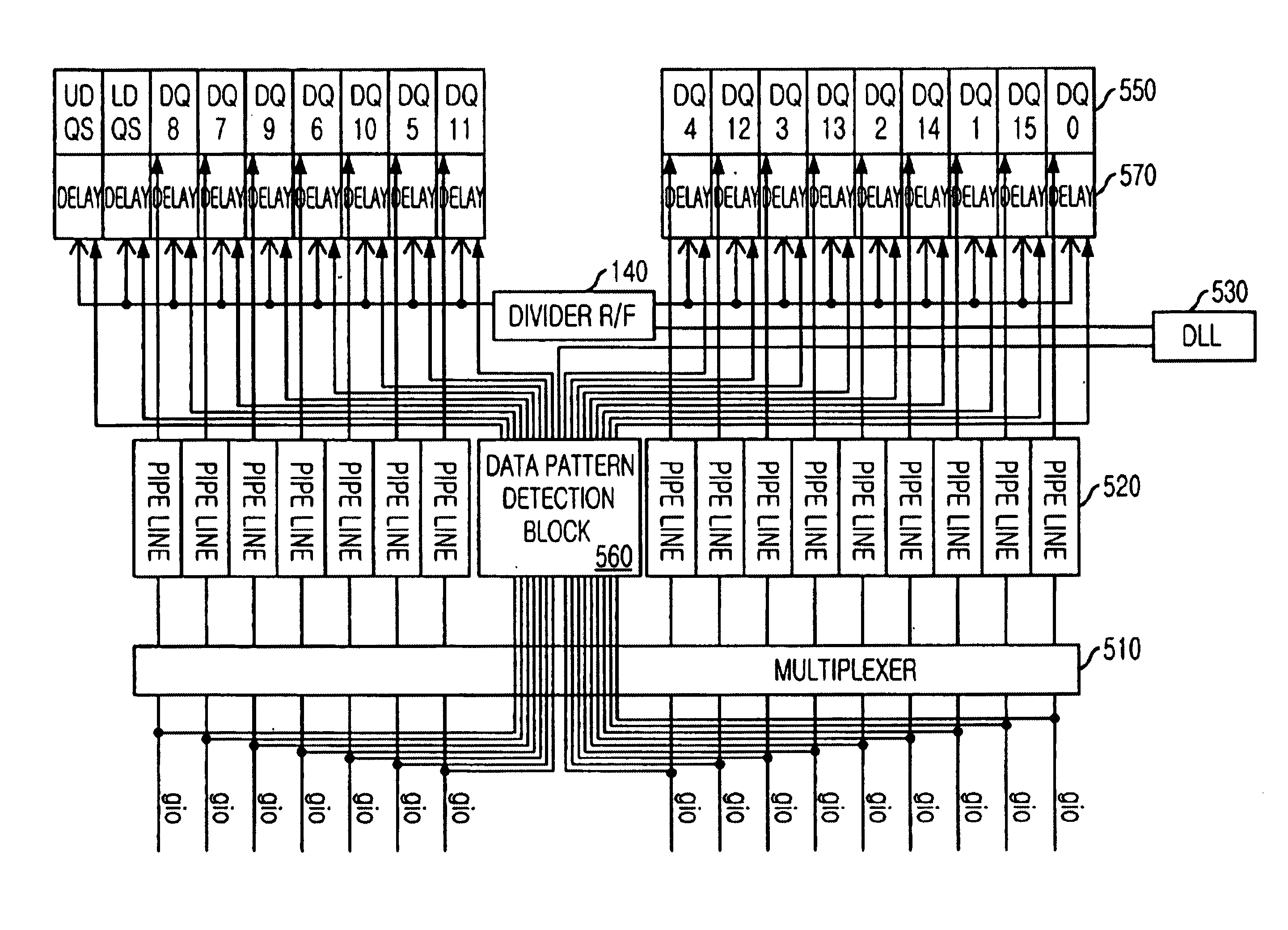
FIG. 5 is a block diagram of a data output path within DRAM chip in accordance with an embodiment of the present invention.

The data output path within the DRAM chip in accordance with the present invention includes a data pattern detection block 560 disposed between global input / output line GIO and delay unit, and a delay compensation block 570 disposed between the data pattern detection block 560 and data output driver 550.

FIG. 6 is a block diagram of an apparatus for reducing a data skew in accordance with an embodiment of the present invention.

Referring to FIG. 6, the apparatus for reducing the data skew includes the data pattern detection block 560 and the delay compensation block 570. The data pattern detection block 560 detects patterns of data loaded on the global input / output line GIO from a memory cell array of DRAM and determines phase delay amount of data inputted to...


PUM


Abstract

An apparatus for minimizing a skew occurring due to a change of data pattern by previously recognizing data pattern before data is outputted from the semiconductor device. The apparatus of compensating for a phase delay in a semiconductor device having a delay locked loop (DLL) for generating DLL clock includes: a data pattern detection block for detecting patterns of data loaded on data line and determining delay compensation amount of the data inputted to data output driver based on the detected data patterns; and a delay compensation block for compensating for phase delay of clock relating to the DLL clock inputted to the data output driver under a control of an output signal of the data pattern detection block.

Description

FIELD OF THE INVENTIONThe present invention relates to a semiconductor device; and, more particularly, to a semiconductor device which is capable of minimizing a skew occurring due to a change of data pattern. Specifically, the present invention relates to a semiconductor device, which is capable of previously recognizing data pattern before data is outputted from the semiconductor device.DESCRIPTION OF RELATED ARTFIG. 1 is a block diagram of a data output path within a conventional DRAM chip.A cell data outputted from DRAM storage cells (memory cell array, not shown) is loaded on a global input / output (GIO) line through a sense amplifier (not shown). Then, the data loaded on the GIO line is transferred to a multiplexer (MUX) 110. The multiplexer 110 supports to select 4, 8 and 16 applications depending on purposes of DRAM.A data outputted from the multiplexer 110 is loaded on a data register 120 (in case of a parallel pipeline scheme, the data register 120 is configured with two or...

Claims


Application Information

Patent Timeline
IPC IPC(8): G11C7/10G06F1/10G11C11/407G11C11/4076H03K5/00H03K5/13H03L7/081
CPCG11C7/1051G11C7/1066G11C7/222G11C7/1072H03L7/0812G11C2207/2254G11C11/407
Inventor KIM, KYUNG-HOON
Owner CONVERSANT INTPROP MANAGEMENT INC
Why Eureka
Try Eureka