Contact printing as second exposure of double exposure attenuated phase shift mask process

a phase shift mask and contact printing technology, applied in the field of semiconductor fabrication, can solve the problems of large burden on optical lithographic processes, difficult resolution of anything smaller than a wavelength, and sub-wavelength lithography, so as to reduce processing times and reduce costs. , the effect of safe increase of the depth of focus

Inactive Publication Date: 2005-03-01
TAIWAN SEMICON MFG CO LTD
View PDF2 Cites 36 Cited by
  • Summary
  • Abstract
  • Description
  • Claims
  • Application Information

AI Technical Summary

Benefits of technology

Embodiments of the invention provide for advantages over the prior art. Using contact printing as the second exposure of the double exposure APSM fabrication process, in lieu of using conventional laser beam writing, provides for decreased processing times. This renders the APSM fabrication process less costly, and thus more advantageous. Contacting printing involves pressing the contact exposure border mask against the resist

Problems solved by technology

Sub-wavelength lithography, however, places large burdens on optical lithographic processes.
Resolution of anything smaller than a wavelength is generally quite difficult.
Pattern fidelity can deteriorate dramatically in sub-wavelength lithography.
Thi

Method used


Image

  • Contact printing as second exposure of double exposure attenuated phase shift mask process
  • Contact printing as second exposure of double exposure attenuated phase shift mask process
  • Contact printing as second exposure of double exposure attenuated phase shift mask process

Examples


Embodiment Construction

In the following detailed description of exemplary embodiments of the invention, reference is made to the accompanying drawings that form a part hereof, and in which is shown by way of illustration specific exemplary embodiments in which the invention may be practiced. These embodiments are described in sufficient detail to enable those skilled in the art to practice the invention. Other embodiments may be utilized, and logical, mechanical, and other changes may be made without departing from the spirit or scope of the present invention. The following detailed description is, therefore, not to be taken in a limiting sense, and the scope of the present invention is defined only by the appended claims.

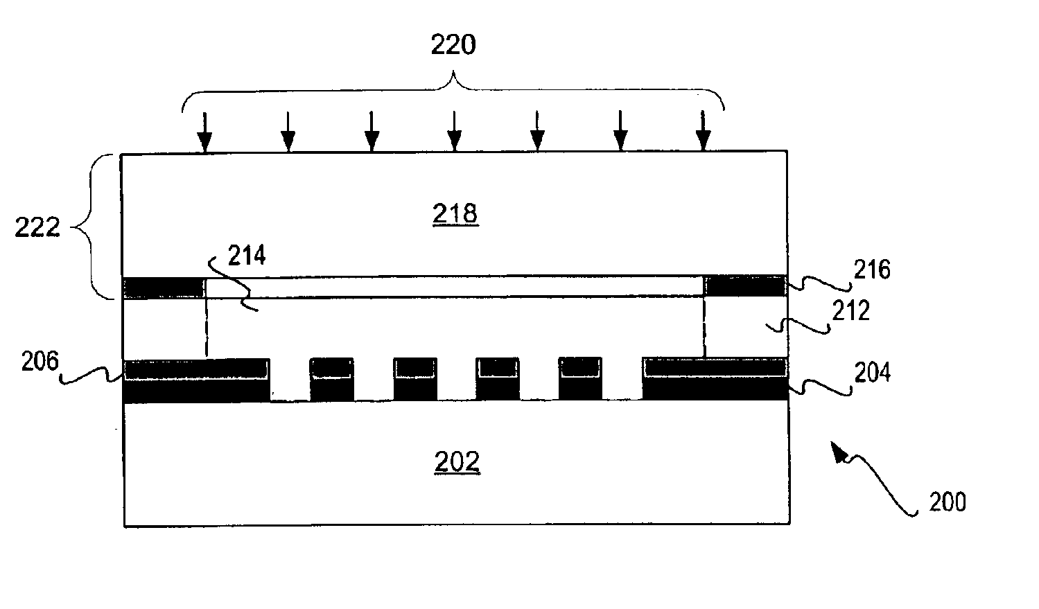
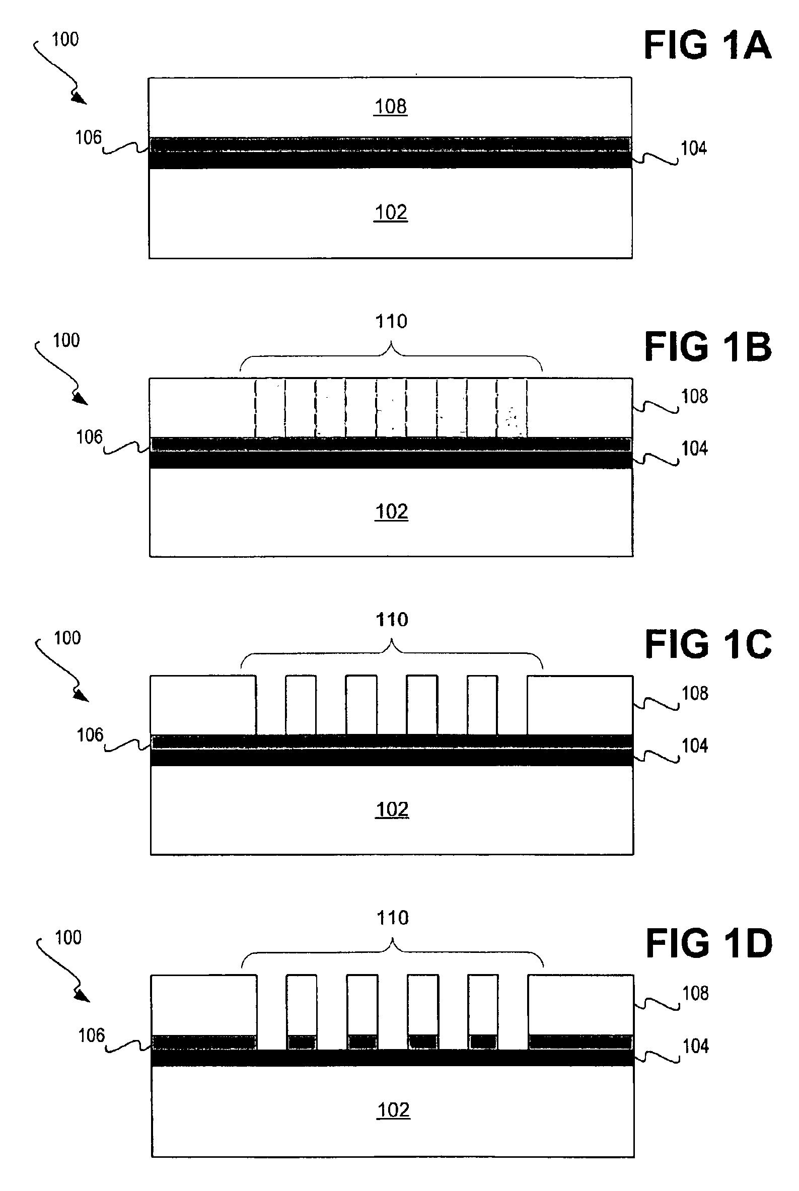
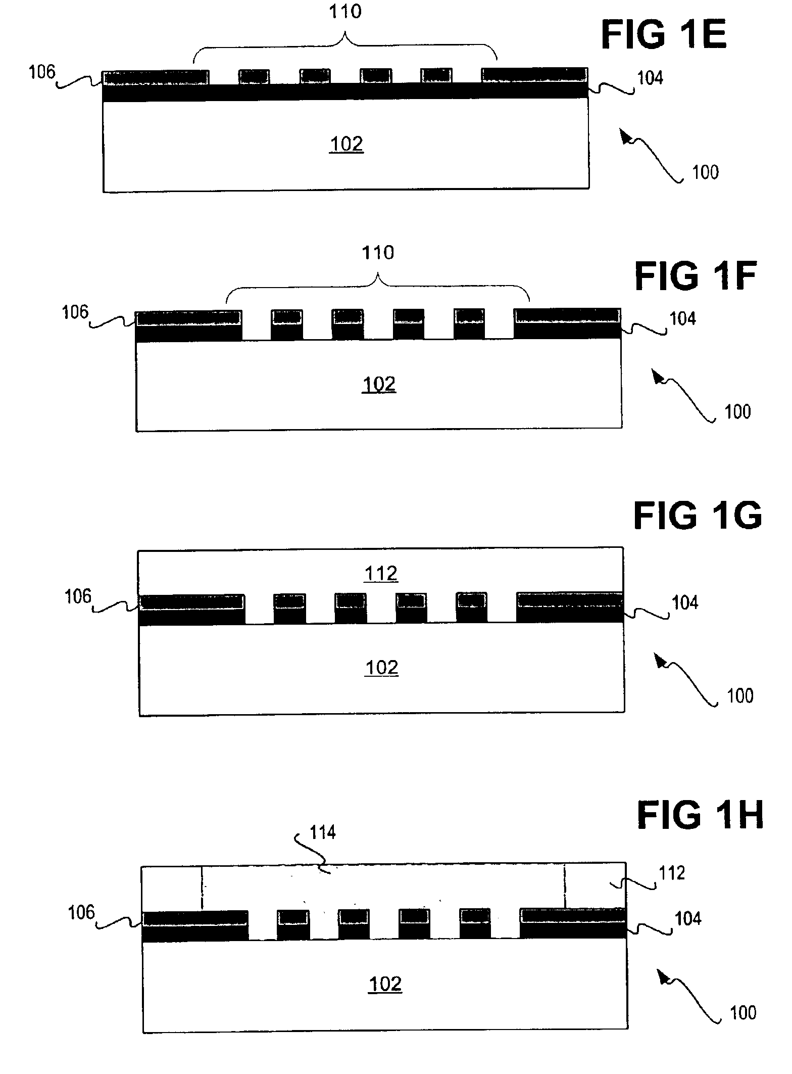
FIGS. 2A-2K illustrate a double exposure attenuated phase shift mask (APSM) fabrication process, according to an embodiment of the invention. In FIG. 2A, the APSM 200 includes a transparent substrate 202, such as quartz. Over the transparent substrate 202 is an attenuated layer 204, such...


PUM


Abstract

Utilizing contact printing as the second exposure within a double exposure attenuated phase shift mask (APSM) fabrication process is disclosed. The process defines the shift pattern within the attenuated layer of the APSM using a first exposure, such as electron beam (e-beam) writing. The attenuated layer may be MoSi, MoSiO, and so on. The process then defines the border pattern within the opaque layer of the APSM using a second exposure. The second exposure employs contact printing, utilizing a contact exposure mask. The contact printing process may align the contact exposure mask over the wafer on which the APSM is fabricated utilizing a camera and an image storage system storing an image of this wafer.

Description

FIELD OF THE INVENTIONThis invention relates generally to semiconductor fabrication, and more particularly to a double exposure attenuated phase shift mask (APSM) process that may be used within such fabrication.BACKGROUND OF THE INVENTIONSince the invention of the integrated circuit (IC), semiconductor chip features have become exponentially smaller and the number of transistors per device exponentially larger. Advanced IC's with hundreds of millions of transistors at feature sizes of 0.25 micron, 0.18 micron, 0.10 micron, and less are becoming routine. Improvement in overlay tolerances in optical photolithography, and the introduction of new light sources with progressively shorter wavelengths, have allowed optical steppers to significantly reduce the resolution limit for semiconductor fabrication far beyond one micron. To continue to make chip features smaller, and increase the transistor density of semiconductor devices, IC's have begun to be manufactured that have features smal...

Claims


Application Information

Patent Timeline
IPC IPC(8): G03F9/00G03F7/20G03C5/00G03F1/08G03F1/14G03B27/02G03F1/32
CPCG03F1/32
Inventor CHANG, CHUNG-HSING
Owner TAIWAN SEMICON MFG CO LTD
Why Eureka
Try Eureka