Semiconductor memory device having the operating voltage of the memory cell controlled

a memory device and integrated circuit technology, applied in the direction of information storage, static storage, digital storage, etc., can solve the problems of inability to operate the circuit, the operation margin of not only reading but also writing becomes smaller, and the sram circuit cannot opera

Inactive Publication Date: 2005-03-01
RENESAS ELECTRONICS CORP
View PDF8 Cites 23 Cited by
  • Summary
  • Abstract
  • Description
  • Claims
  • Application Information

AI Technical Summary

Benefits of technology

The operation margin for reading and writing is controlled by using a semiconductor memory which comprises an array of a plurality of static memory cells, a peripheral circuit for controlling the above memory array, and a circuit for changing the operating voltage of the above memory array according to the threshold voltage of a transistor in each of the above static memory cells. Since the operation margin changes according to the performance of the transistor, after the production of an LSI or during the operation of the LSI, the threshold voltage of the transistor is detected to determine the optimum operating voltage for the memory array so as to apply the optimum voltage to the memory array. As alternative means, the characteristics of the transistor after the production of an LSI are detected to adjust the operating voltage for the memory array and further substrate potentials for transistors in the memory cell in order to vary the threshold value of transistors constituting the memory cell. The line suppling the operating voltage of the memory array and the line suppling the operating voltage of the peripheral circuit are separated from each other, and a voltage corresponding to the threshold voltage of the transistors in the memory array is added to the operating voltage of the peripheral operating voltage to the memory array. Thus, different voltages can be applied to the memory array and the peripheral circuit.

Problems solved by technology

When the threshold voltage of the transistor is reduced, the static noise margin (SNM) which is the operation margin for reading the data of a SRAM memory cell becomes small, thereby making it difficult to operate the circuit.
When the operating voltage is further reduced, the operation margin for not only reading but also writing becomes smaller with the result that the SRAM circuit does not operate.

Method used


Image

  • Semiconductor memory device having the operating voltage of the memory cell controlled
  • Semiconductor memory device having the operating voltage of the memory cell controlled
  • Semiconductor memory device having the operating voltage of the memory cell controlled

Examples


embodiment 1

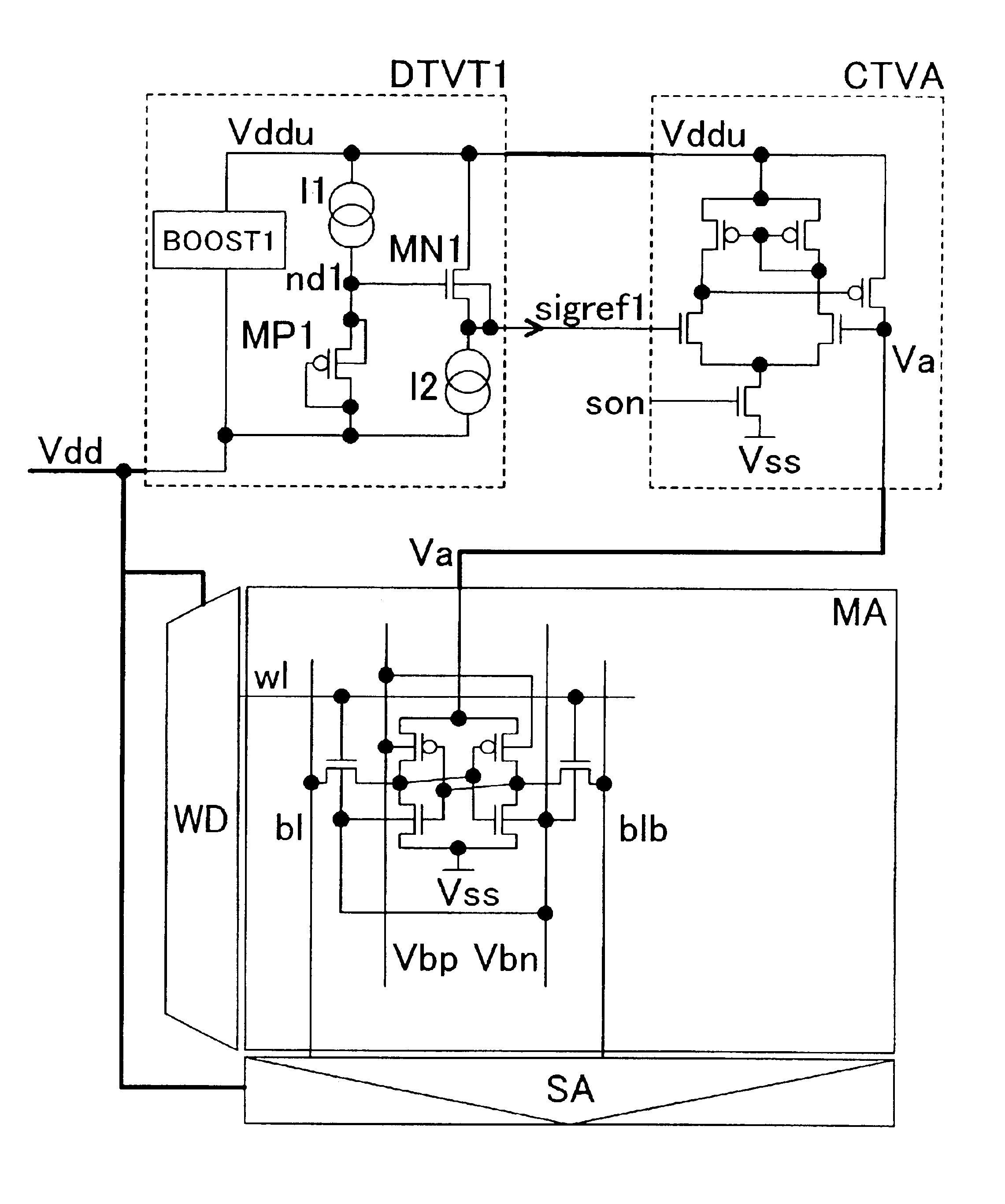
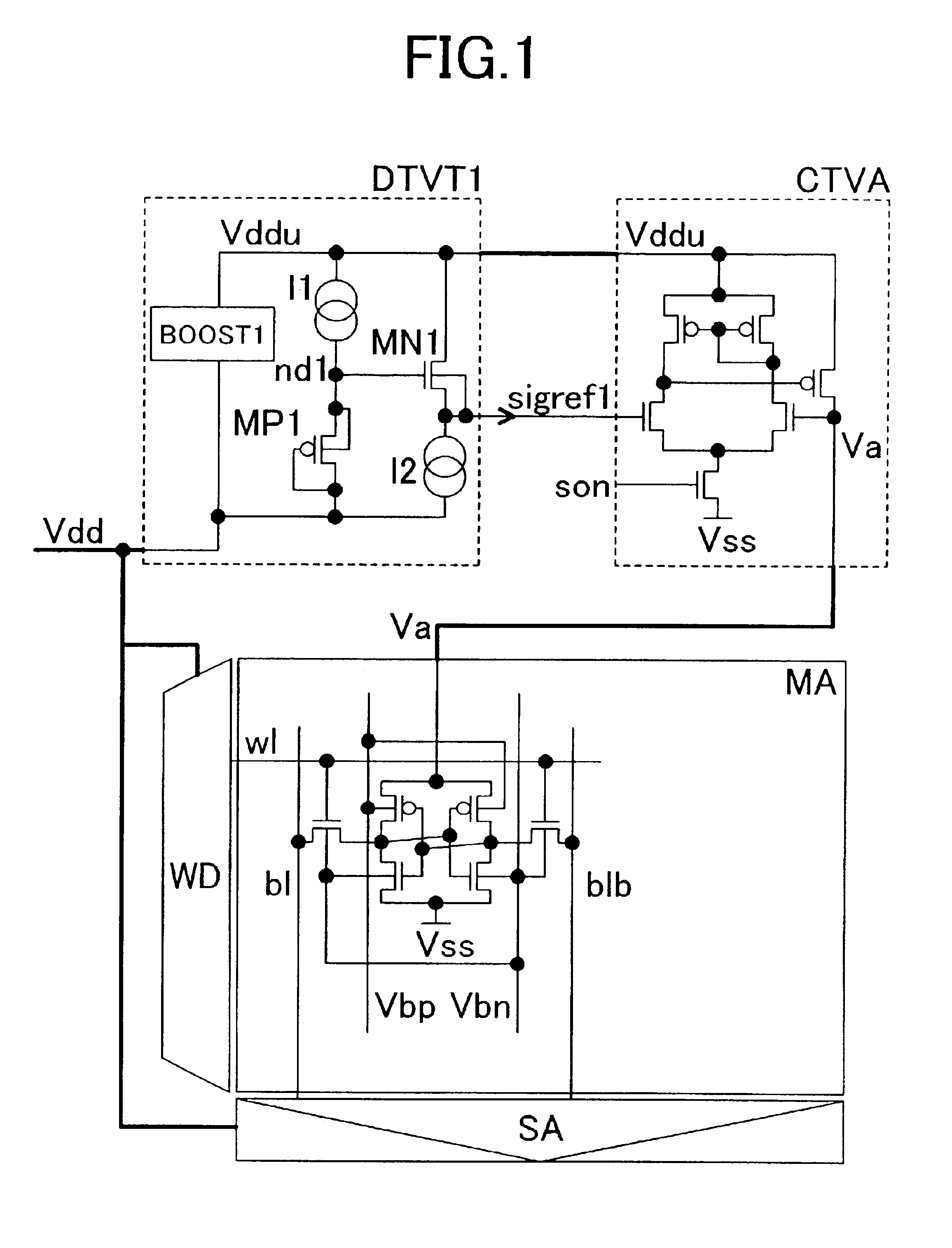
FIG. 1 schematically shows a SRAM circuit and its power constitution according to the present invention. In FIG. 1, MA is an array of SRAM memory cells, WD is a circuit for controlling the word line, a word driver or a row address decoder, SA is a circuit for controlling the bit line, a sense amplifier, precharging circuit or column decoder, DTVT1 is a circuit which detects the threshold voltage of pMOS and nMOS transistors and generates reference potential signal sigref1 for generating the operating operating voltage of the memory array, and CTVA is a power circuit for outputting an operating voltage Va of the memory array by increasing or reducing the operating voltage Vdd based on the signal sigref1 from DTVT1. W1 in the memory array MA is the word line of a memory cell, b1 and b1b are bit lines, Vss is a ground potential line, Vbp is a node connected to the substrate electrode of a pMOS transistor in the memory cell, and Vbn is a node connected to the substrate electrode of nMOS...

embodiment 2

FIG. 7 schematically shows another SRAM circuit and its voltage control constitution. In FIG. 7, MA is an array of SRAM memory cells, WD is a circuit for controlling the word line, a word driver, and row address decoder, SA is a circuit for controlling the bit line, a sense amplifier, precharger circuit and column decoder, BOOST 2 is a booster circuit for increasing Vdd to generate voltage Vddu, CTVA is a voltage controlling circuit for outputting an operating voltage Va for the memory array based on a reference potential signal sigref2, DREG1 is a circuit for outputting a reference potential specified by a reference potential selection signal swcont1, and DTVT2 is a circuit for outputting a reference potential selection signal swcont1 in accordance with the threshold voltages of transistors. During the operation of this circuit, the threshold voltage detection circuit DTVT2 outputs a signal swcont1 for selecting the optimum voltage for the memory array based on the threshold voltag...

embodiment 3

FIG. 11 schematically shows still another SRAM circuit according to the present invention. In FIG. 11, MA is an array of SRAM memory cells, WD is a circuit for controlling the word line, a word driver, row address decoder, SA is a circuit for controlling the bit line, a sense amplifier, precharger circuit and column decoder, DTVT3 is a circuit for detecting the threshold voltages of transistors and generating a reference potential signal sigref3 for generating an operating voltage for the memory array and reference potential signals sigref4 and sigref5 for generating substrate potentials for the memory array, CTVA is a voltage control circuit for increasing or reducing the operating voltage Vdd based on the signal sigref3 from DTVT3 to apply an operating voltage Va to the memory array, and CTVBB is a circuit for generating Vbn and Vbp which are substrate potentials for the memory array in response to the signals sigref4 and sigref5 from DTVT3. Vbn is a potential for p well which is ...


PUM


Abstract

An SRAM circuit which can be operated at a reduced operation margin, especially at a low operating voltage by increasing or optimizing the operation margin of the SRAM circuit. The threshold voltage of the produced transistor in the SRAM circuit is detected to compare the operating voltage of a memory cell with the operating voltage of a peripheral circuit in order to adjust it to the optimum value, and the substrate bias voltage is further controlled.

Description

BACKGROUND OF THE INVENTION1. Field of the InventionThe present invention relates to a semiconductor integrated circuit having a static memory (SRAM) circuit integrated on a semiconductor chip. More specifically, it relates to constitution for reducing the operating voltage of a SRAM integrated circuit device.2. Description of Related ArtJP-A 139779 / 1994 discloses a circuit for comparing the threshold voltage of the transistor of a memory cell with a preset reference voltage and generating a substrate bias voltage so that the threshold voltage becomes equal to the reference voltage. JP-A268574 / 2000 discloses a circuit for changing a substrate bias voltage using signals from a threshold value detection circuit and from a voltage detection circuit for transistors to approximate the threshold value of the transistor of a memory cell to a preset value.The operating voltages of large scale integrated circuits (LSIs) are decreasing due to reductions in the power consumption of LSIs and th...

Claims


Application Information

Patent Timeline
Patent Type & Authority Patents(United States)
IPC IPC(8): G11C11/419G11C11/417G11C11/413G11C11/4193G11C29/02
CPCG11C5/146G11C5/147G11C11/412G11C11/413G11C11/419G11C29/02G11C29/021G11C29/028G11C11/417G11C11/41G11C2029/0409
Inventor YAMAOKA, MASANAOOSADA, KENICHI
Owner RENESAS ELECTRONICS CORP
Why Eureka
Try Eureka