Semiconductor integrated circuit device having body biasing circuit for generating forward well bias voltage of suitable level by using simple circuitry

a technology of integrated circuit and biasing circuit, which is applied in the direction of pulse generator, pulse technique, electric pulse generator details, etc., can solve the problems of increasing power consumption, increasing the subthreshold leakage current, and reducing the threshold voltage of the mos transistor

Inactive Publication Date: 2005-03-08
RENESAS ELECTRONICS CORP
View PDF3 Cites 50 Cited by
  • Summary
  • Abstract
  • Description
  • Claims
  • Application Information

AI Technical Summary

Benefits of technology

An object of the present invention is to provide a semiconductor integrated circuit device having a body biasing circuit that can generate a forward body (well) bias voltage of a suitable level by using simple circuitry.

Problems solved by technology

However, as the reduced supply voltage results in a lower operating speed, if the power consumption is to be reduced without compromising the operating speed, the threshold voltage of the MOS transistors has had to be reduced.
Reducing the threshold voltage of the MOS transistors leads to faster switching operation of the MOS circuit, but this in turn results in an increase in subthreshold leakage current, and hence an increase in power consumption.
However, application of a forward bias voltage to the well (body) involves other problems such as an increase in chip area due to the addition of a bias voltage generating circuit.

Method used


Image

  • Semiconductor integrated circuit device having body biasing circuit for generating forward well bias voltage of suitable level by using simple circuitry
  • Semiconductor integrated circuit device having body biasing circuit for generating forward well bias voltage of suitable level by using simple circuitry
  • Semiconductor integrated circuit device having body biasing circuit for generating forward well bias voltage of suitable level by using simple circuitry

Examples


Embodiment Construction

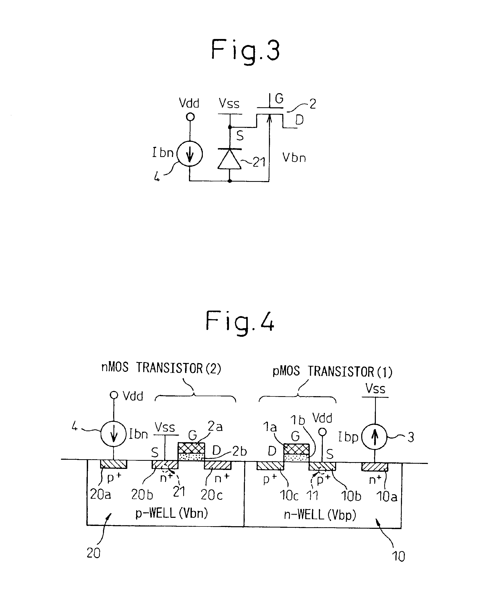
Before proceeding to the detailed description of the semiconductor integrated circuit device according to the present invention, the prior art semiconductor integrated circuit device and its associated problem will be described first, with reference to the drawings.

For high-speed and low-power operation of CMOS circuits, a technique that applies a forward bias voltage to the body (well) of a MOS transistor has been attracting attention in recent years.

Specifically, in the prior art there is proposed a semiconductor integrated circuit device (CMOS chip) that achieves both high-speed operation and low power consumption by applying a forward body bias FBB during active operation and a zero body bias ZBB in standby mode (for example, refer to S. Narendra et al., “1.1V 1 GHz Communications Router with On-Chip Body Bias 150 nm CMOS,” ISSCC 2002 / SESSION 16 / HIGH SPEED I / O 16.4,pp. 270, 271, 466: Feb. 5, 2002).

In the prior art, there is also proposed a semiconductor integrated circuit device...


PUM


Abstract

A semiconductor integrated circuit device has a MISFET and a body biasing circuit. The MISFET has a source electrode and a drain electrode of a first conductivity type and a gate electrode, and the MISFET is formed in a well of a second conductivity type. The body biasing circuit generates a voltage in the well by passing a prescribed current in a forward direction into a diode which is formed from the well and the source electrode of the MISFET.

Description

CROSS REFERENCE TO RELATED APPLICATIONThis application is based upon and claims the benefit of priority from the prior Japanese Patent Application Nos. 2002-211536, filed on Jul. 19, 2002 and 2003-019271,filed on Jan. 28, 2003, the entire contents of which are incorporated herein by reference.BACKGROUND OF THE INVENTION1. Field of the InventionThe present invention relates to a semiconductor integrated circuit device and, more particularly, to a semiconductor integrated circuit device comprising a high-speed, low-voltage operating MISFET.2. Description of the Related ArtRecently, the widespread use and the increased functionality of portable information apparatuses such as portable telephones and portable PDAs (Personal Digital Assistants) have been driving the need to further increase the operating speed and reduce the power consumption of semiconductor integrated circuit devices constructed from MOSFETs (Metal-Oxide-Semiconductor Field Effect Transistors, or more broadly, MISFETs ...

Claims


Application Information

Patent Timeline
Patent Type & Authority Patents(United States)
IPC IPC(8): H01L27/085H01L27/02H01L27/07H01L27/092H03K19/017H03K17/041H03K19/003H03K19/01H03K17/04
CPCH01L27/0218H01L27/0727H01L27/092H01L27/0928H03K17/04106H03K19/00384H03K19/01707H01L2924/0002Y10S257/901H01L2924/00
Inventor ISHIBASHI, KOICHIROYAMASHITA, TAKAHIRO
Owner RENESAS ELECTRONICS CORP
Why Eureka
Try Eureka