Layout technique for C3MOS inductive broadbanding

Inactive Publication Date: 2005-03-08
AVAGO TECH INT SALES PTE LTD
View PDF101 Cites 11 Cited by
  • Summary
  • Abstract
  • Description
  • Claims
  • Application Information

AI Technical Summary

Benefits of technology

According to one aspect of the invention, an improved cell layout for a C3MOS circuit with inductive broadbanding effe

Problems solved by technology

The layout of the interconnects is a complex geometrical problem.
However, in high frequency ICs the layout must also account for electromagnetic effects, which cause parasitic resistance and capacitance which can degrade the performance of the IC.
Since the length of the interconnects is directly proportional to thei

Method used


Image

  • Layout technique for C3MOS inductive broadbanding
  • Layout technique for C3MOS inductive broadbanding
  • Layout technique for C3MOS inductive broadbanding

Examples


Embodiment Construction

In one embodiment of the invention, the circuit elements are fabricated utilizing ultra-high-speed logic circuitry implemented in silicon complementary metal-oxide-semiconductor (CMOS) process technology. A distinction is made herein between the terminology “CMOS process technology” and “CMOS logic.” CMOS process technology as used herein refers generally to a variety of well established CMOS fabrication processes that form a field-effect transistor over a silicon substrate with a gate terminal typically made of polysilicon material disposed on top of an insulating material such as silicon dioxide.

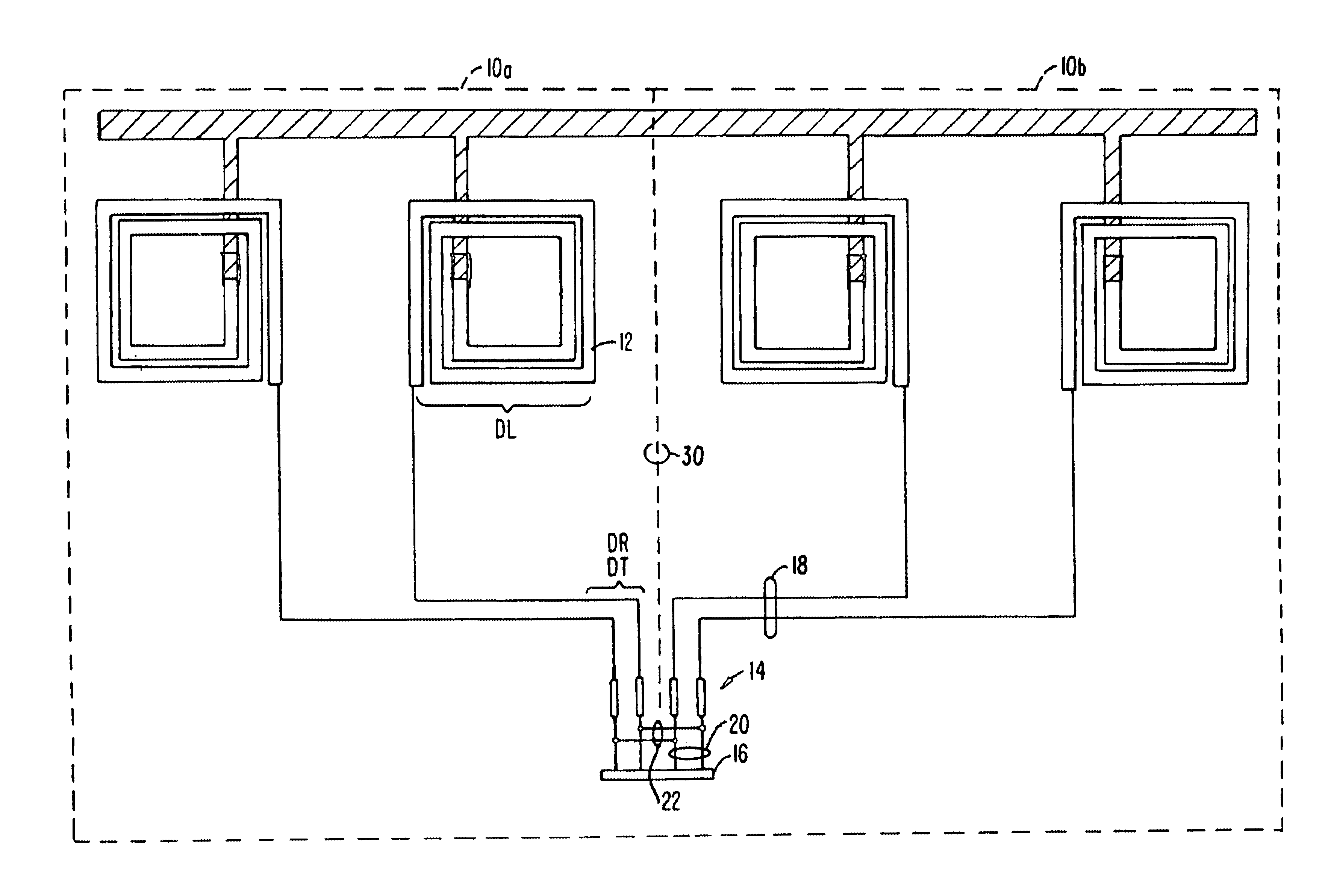
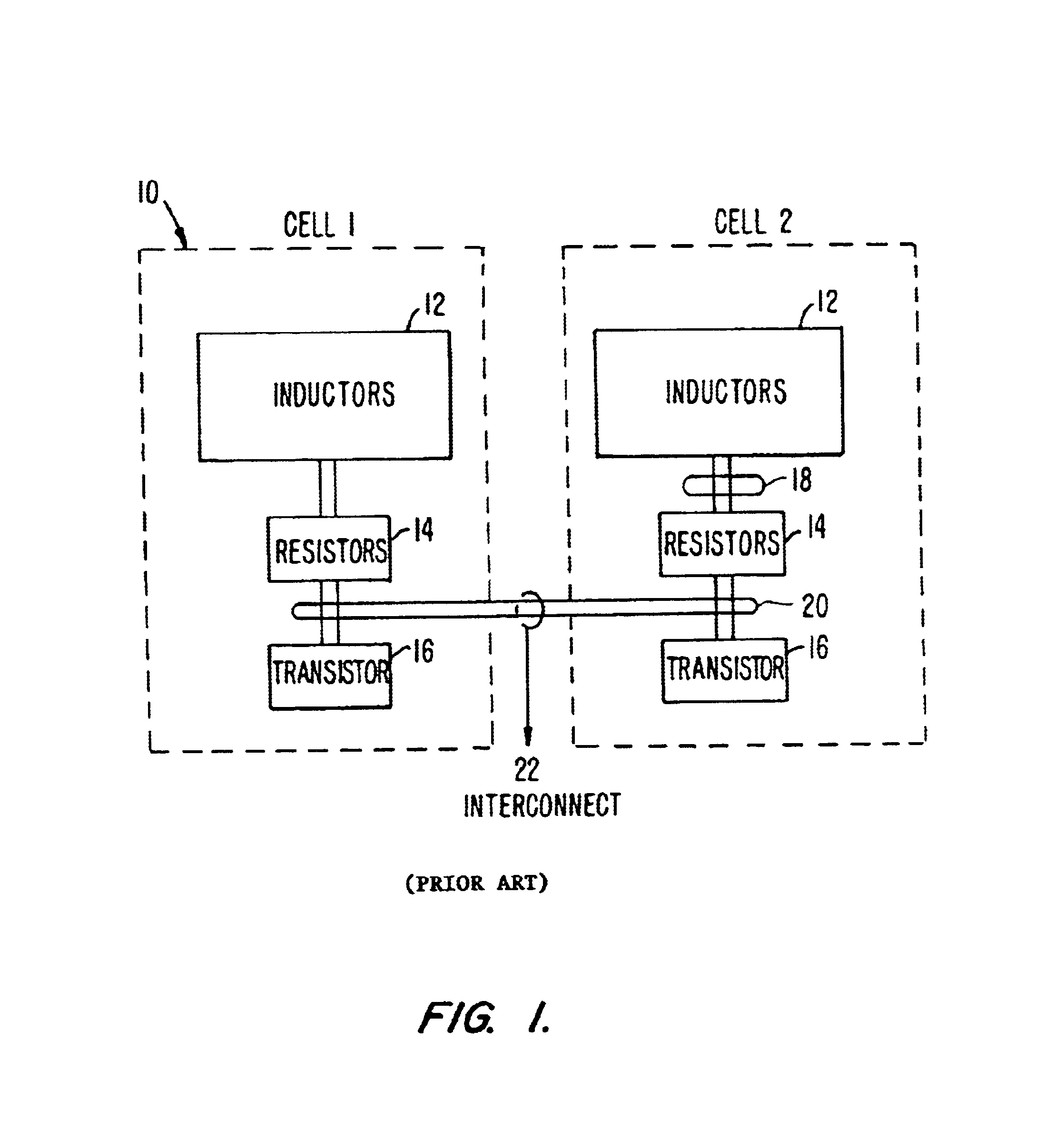
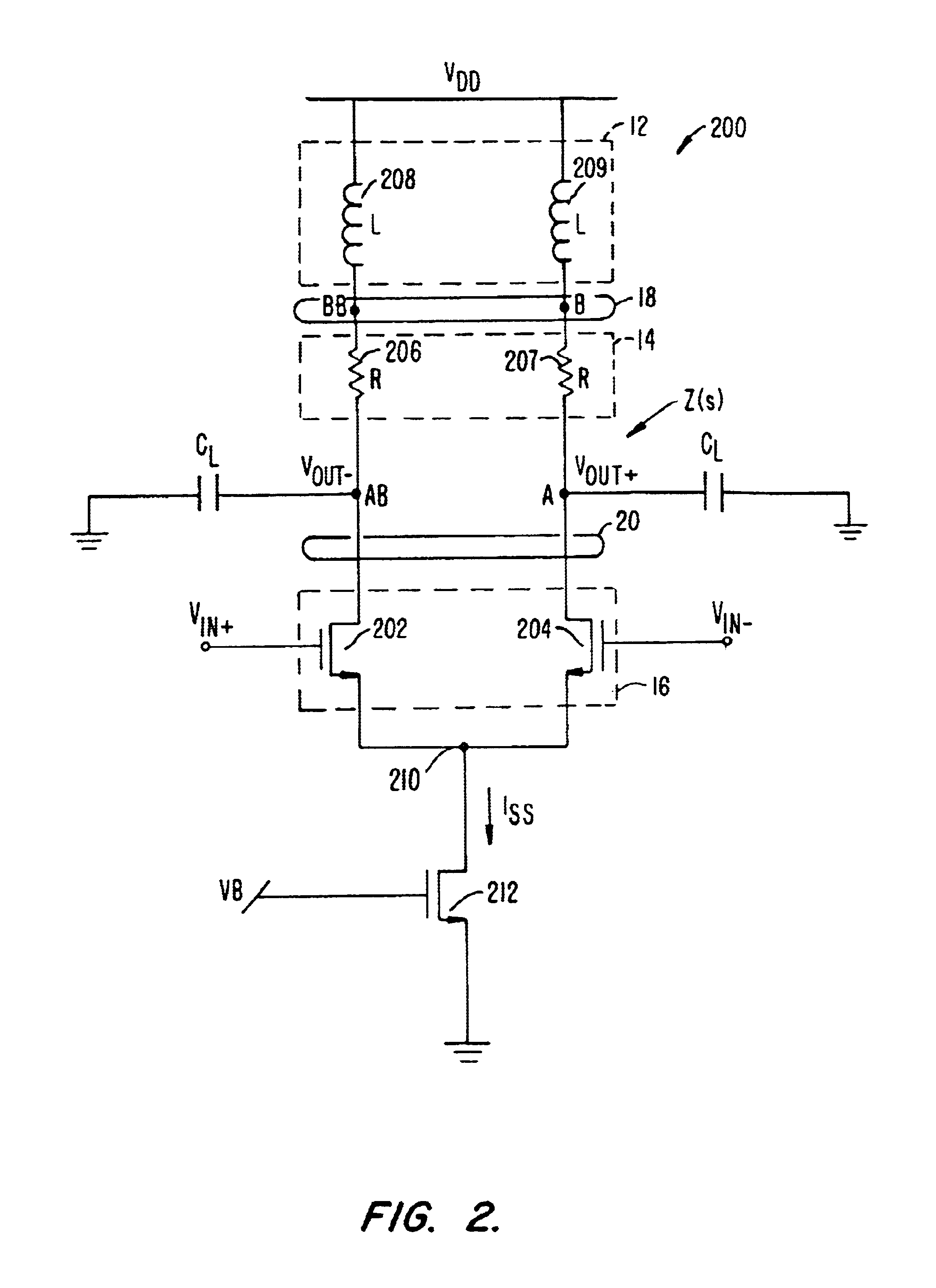
FIG. 2 depicts a buffer circuit fabricated utilizing, by way of example, not limitation, C3MOS technology which is described in detail in the above-referenced patent application. It is to be understood that the present invention is useful in many contexts and is not limited to particular circuit designs.

FIG. 2 is a schematic diagram of a buffer circuit utilizing inductive broadbanding, ill...


PUM


Abstract

An improved cell layout for a C3MOS circuit with inductive broadbanding positions the inductor at a distance from the active region to improve isolation and aligns the edges of the resistor, inductor, and transistor regions near the common edge of adjacent cells to decrease the length of the cell-to-cell interconnect lines.

Description

BACKGROUND OF THE INVENTIONThe design of an integrated circuit (IC) requires that a layout be designed which specifies the arrangement of the various circuit components on the major surface of a semiconductor substrate, for example a silicon crystal.Since many circuit elements are repeatedly utilized, these circuit elements are reduced to cells. The layout can be generated by arranging the cells and connecting them using conductive interconnects. Layout is usually performed utilizing sophisticated software tools well-known to persons of skill in the art.The layout of the interconnects is a complex geometrical problem. However, in high frequency ICs the layout must also account for electromagnetic effects, which cause parasitic resistance and capacitance which can degrade the performance of the IC.FIG. 1 depicts the standard design of a cell 10, a layout of two cells, and the interconnection of the cells where each cell 10 includes an inductor region 12, a resistor region 14, and a t...

Claims


Application Information

Patent Timeline
IPC IPC(8): H01L27/06H03K19/017H03K19/01
CPCH01L27/0629H03K19/01707H01L2924/0002H01L2924/00
Inventor MOMTAZ, AFSHIN D.GREEN, MICHAEL M.
Owner AVAGO TECH INT SALES PTE LTD
Why Eureka
Try Eureka