Adjustable differential input and output drivers

a technology of input and output drivers and differential signals, which is applied in logic circuit coupling/interface arrangements, pulse techniques, baseband system details, etc., can solve the problems of unoptimized common-mode voltage for input and output drivers, unsatisfactory power losses, etc., and achieve the optimization of differential signal paths associated with these drivers. performance and power consumption, the effect of reducing the overall resistance of the circui

Active Publication Date: 2005-03-08
TAHOE RES LTD
View PDF10 Cites 49 Cited by
  • Summary
  • Abstract
  • Description
  • Claims
  • Application Information

AI Technical Summary

Benefits of technology

In a suitable combined resistor-current-source arrangement, the current source may be implemented as multiple current mirror branch sections, each having an associated series-connected resistor. Control transistors can be used to connect or disconnect desired branches from the circuit. When more branches are connected, the current contributions from those branches increase the overall current source current, while the additional parallel resistance contribu

Problems solved by technology

This may lead to undesirable power losses.
Moreover, when the common-mode biases from each end of a link do n

Method used


Image

  • Adjustable differential input and output drivers
  • Adjustable differential input and output drivers
  • Adjustable differential input and output drivers

Examples


Embodiment Construction

The present invention relates to adjustable differential input and output drivers. The invention also relates to the integrated circuits and systems with which such differential input and output drivers are used and methods for controlling and using these components.

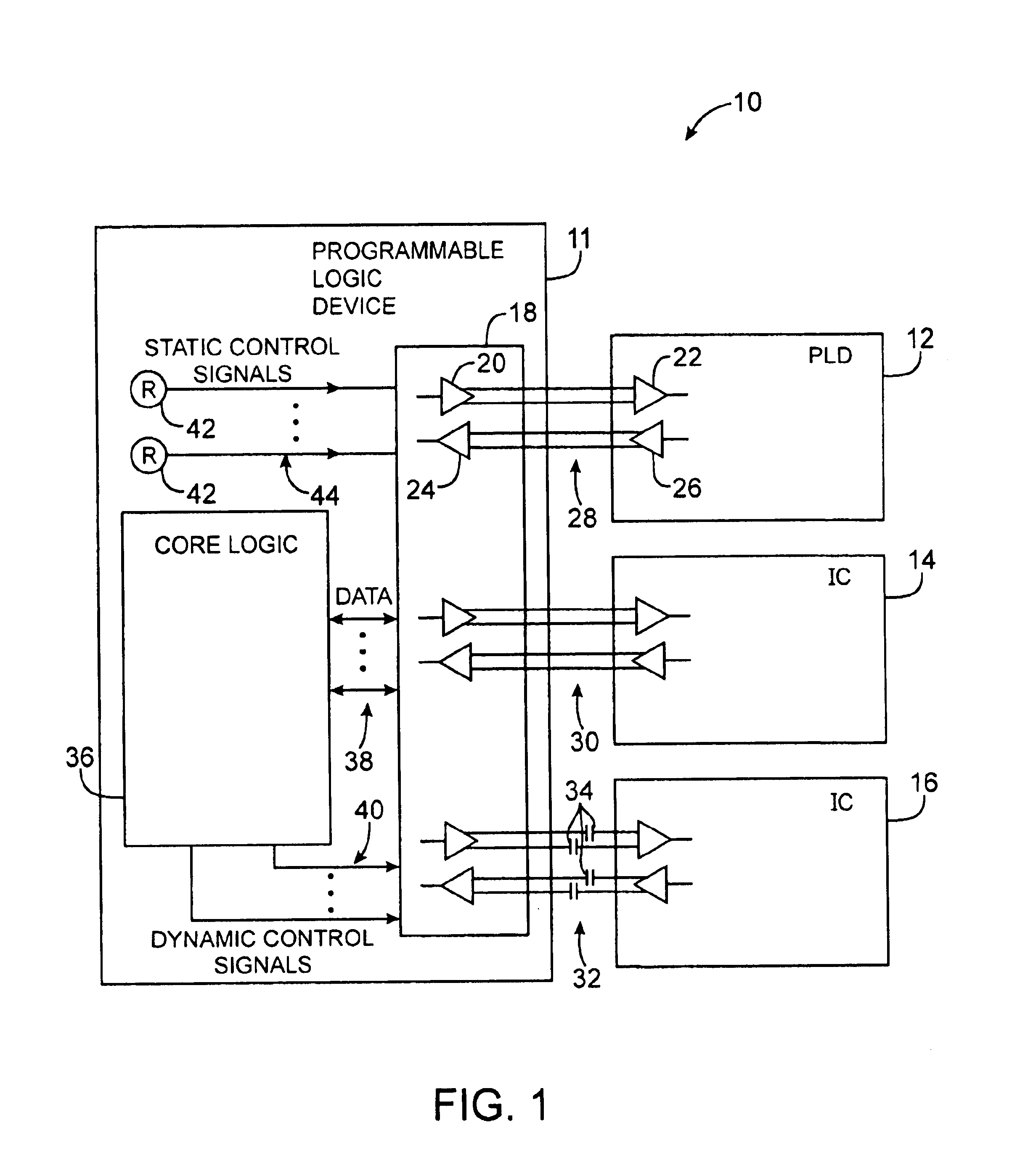
An illustrative system 10 in accordance with the present invention is shown in FIG. 1. In the illustrative system of FIG. 1, a programmable logic device integrated circuit 11 is in communication with another programmable logic device 12 and integrated circuits 14 and 16. Some of the communications in system 10 such as communications between programmable logic device 11 and other integrated circuit components may be made using single-ended input and output drivers. With single-ended input and output drivers, data signals are referenced to ground potential.

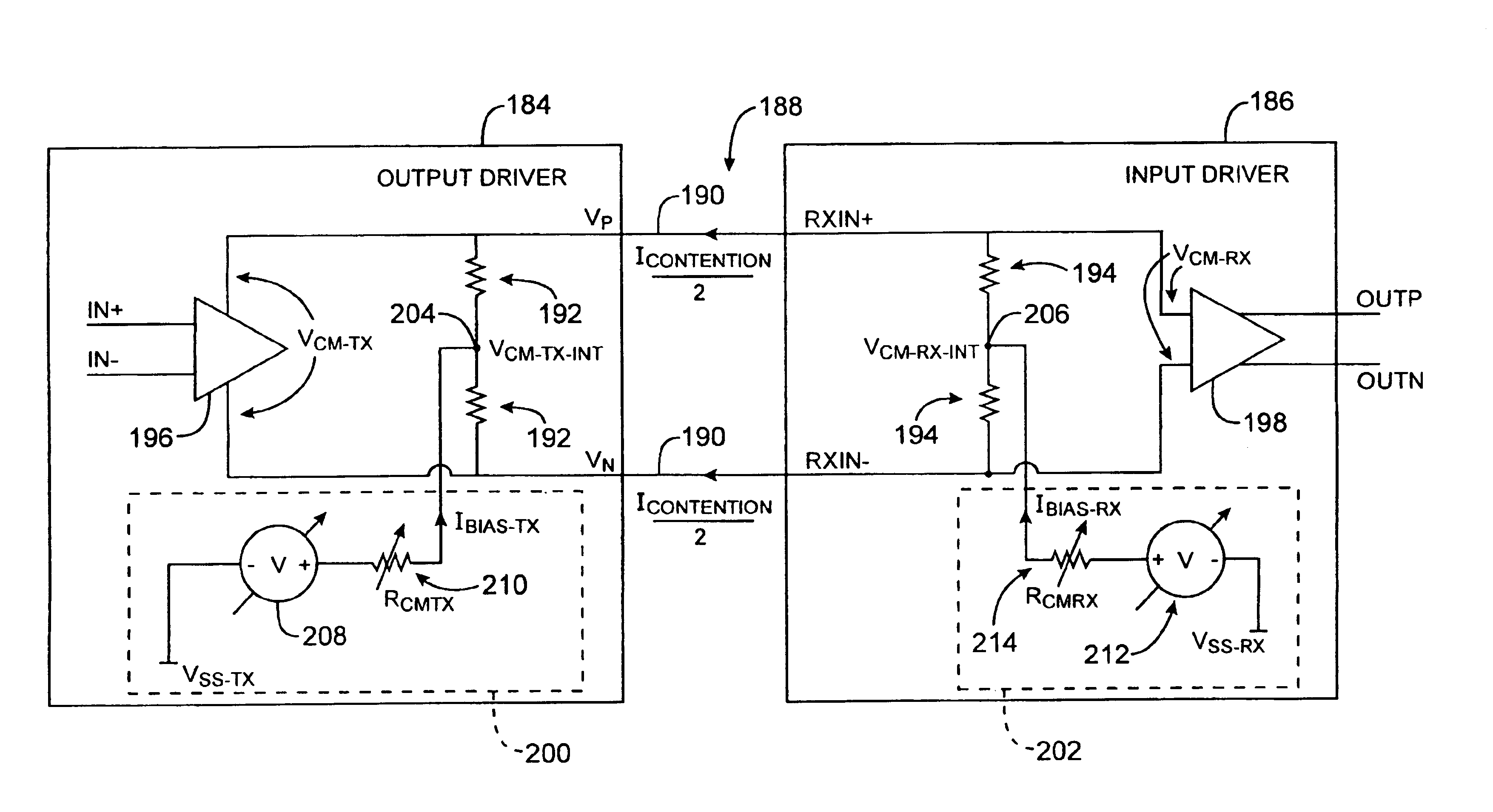
In the example of FIG. 1, the communications links between the components of the system are differential communications links. In each differential signal path, the sign...


PUM


Abstract

Systems and methods are provided using common-mode-voltage bias circuitry to make common-mode-voltage adjustments to differential driver circuitry in integrated circuit differential communications links. Adjustable bias circuitry may be controlled using static and dynamic control signals. Dynamic control signals can be produced by core logic on a programmable logic device or other integrated circuit. Static control signals can be produced by programmable elements. Bias circuit adjustments made at one end of a differential link can be used to improve performance at either end of the link or can be used to improve power consumption or to balance power and performance considerations. The same integrated circuit design can be used in both AC-coupled and DC-coupled environments. The bias circuitry can be formed from an adjustable current source and adjustable resistor. The current source and adjustable resistors can be controlled by the same control signals.

Description

BACKGROUND OF THE INVENTIONThis invention relates to integrated circuit input-output (I / O) circuitry, and more particularly, to adjustable differential integrated circuit input and output drivers for AC-coupled and DC-coupled communications links.Input-output (I / O) circuitry is used on integrated circuits as an interface between the circuitry on the integrated circuit and external components. Input-output circuitry typically includes either single-ended or differential input drivers and single-ended or differential output drivers.Single-ended drivers are used to handle single-ended signals—i.e., signals that are referenced to ground.Differential drivers are used to handle differential signals, which are carried on pairs of conductors. Differential signals are referenced to each other, rather than a source of ground potential. One of the differential signals in each differential signal pair may be labeled “positive” and the other one of the differential signals in that pair may be la...

Claims


Application Information

Patent Timeline
IPC IPC(8): H03K19/0185H04L25/02
CPCH04L25/0276H03K19/018564
Inventor WONG, WILSONSHUMARAYEV, SERGEY
Owner TAHOE RES LTD
Why Eureka
Try Eureka