Method to alter chalcogenide glass for improved switching characteristics

a technology of chalcogenide glass and switching characteristics, applied in the field of resistance variable memory element having improved switching characteristics, can solve the problems of volatile ram devices, shrinking the size of each element, loss of stored data, etc., and achieves tighter rigid glass matrix, improved switching characteristics and data retention

Inactive Publication Date: 2005-03-15
ROUND ROCK RES LLC
View PDF221 Cites 28 Cited by
  • Summary
  • Abstract
  • Description
  • Claims
  • Application Information

AI Technical Summary

Benefits of technology

In its structure aspect, the invention provides a metal containing resistance variable material having

Problems solved by technology

Typically, RAM devices are volatile, in that stored data is lost once the power source is disconnected or removed.
Accordingly, the size of each element has been shrinking, which in the case of DRAMs also shortens the element's data holding time.
However, with increasing element number and densi

Method used


Image

  • Method to alter chalcogenide glass for improved switching characteristics
  • Method to alter chalcogenide glass for improved switching characteristics
  • Method to alter chalcogenide glass for improved switching characteristics

Examples


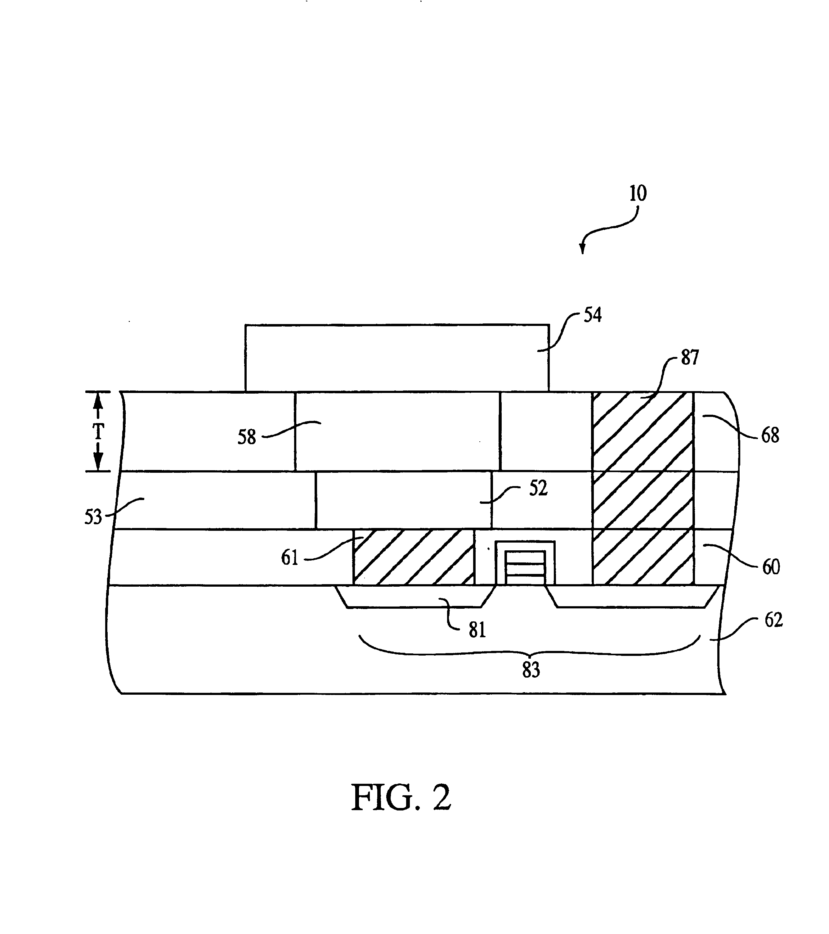
Embodiment Construction

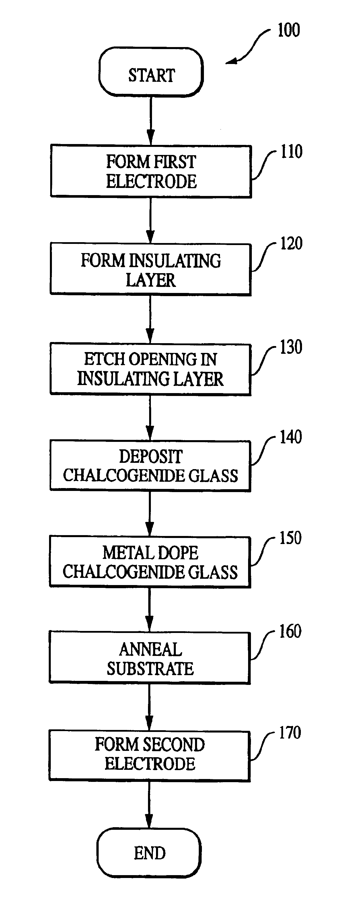
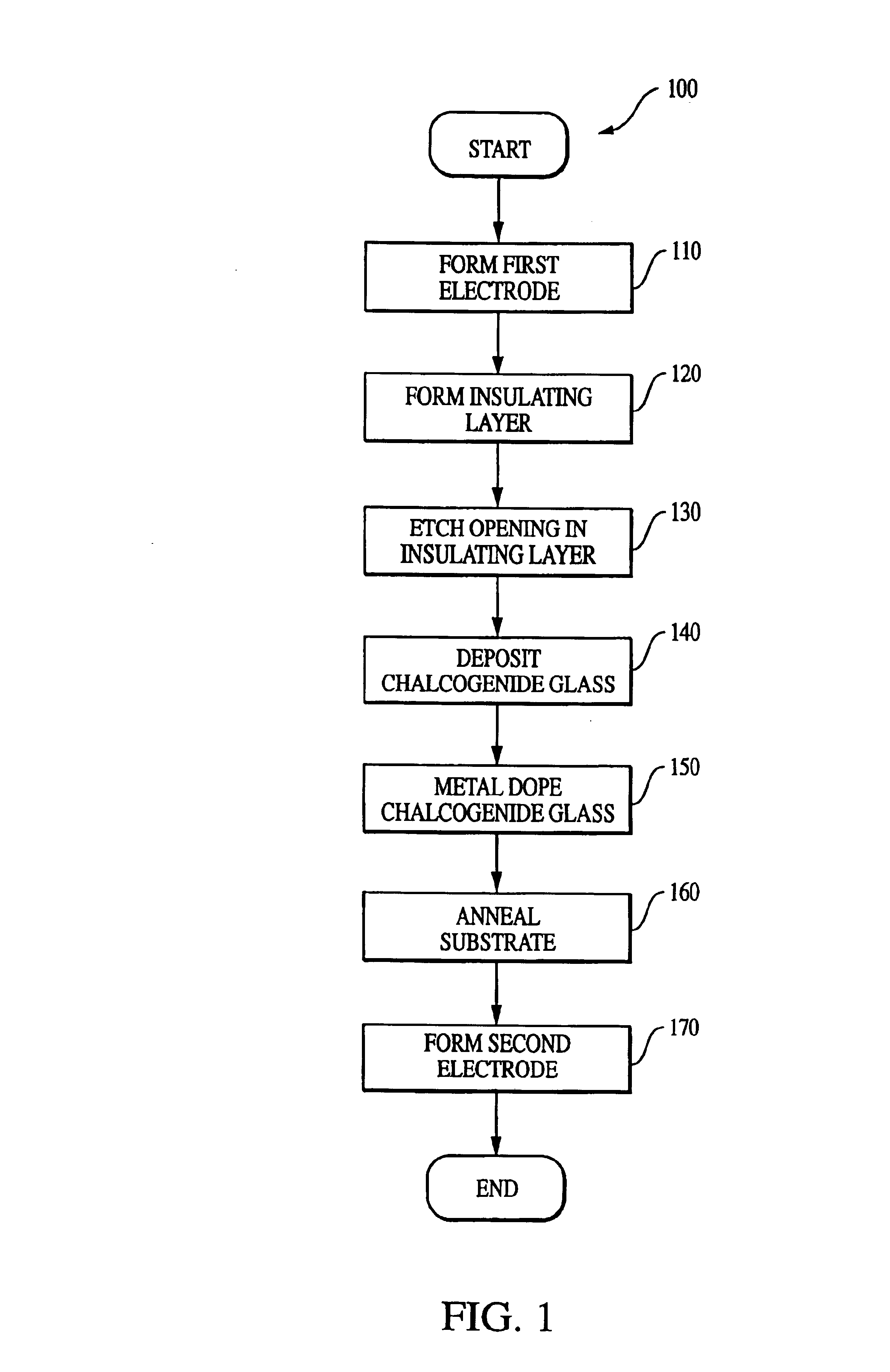
In the following detailed description, reference is made to various specific structural and process embodiments of the invention. These embodiments are described with sufficient detail to enable those skilled in the art to practice the invention. It is to be understood that other embodiments may be employed, and that various structural, logical and electrical changes may be made without departing from the spirit or scope of the invention.

The term “substrate” used in the following description may include any supporting structure including but not limited to a semiconductor substrate that has an exposed substrate surface. Structure should be understood to include silicon-on-insulator (SOI), silicon-on-sapphire (SOS), doped and undoped semiconductors, epitaxial layers of silicon supported by a base semiconductor foundation, and other semiconductor structures. When reference is made to a substrate or wafer in the following description, previous process steps may have been utilized to fo...


PUM


Abstract

The present invention is related to methods of fabricating a resistance variable memory element and a device formed therefrom having improved switching characteristics. According to an embodiment of the present invention a resistance variable material memory element is annealed to remove stoichiometric amounts of a component of the resistance variable material. According to another embodiment of the present invention a silver-germanium-selenide glass is annealed for a duration of about 10 minutes in the presence of oxygen to drive off selenium and increase the rigidity of the glass.

Description

FIELD OF THE INVENTIONThe present invention relates to the field of random access memory (RAM) devices formed using a resistance variable material, and in particular to a resistance variable memory element having improved switching characteristics.BACKGROUND OF THE INVENTIONA well known semiconductor component is semiconductor memory, such as a random access memory (RAM). RAM permits repeated read and write operations on memory elements. Typically, RAM devices are volatile, in that stored data is lost once the power source is disconnected or removed. Non-limiting examples of RAM devices include dynamic random access memory (DRAM), synchronized dynamic random access memory (SDRAM) and static random access memory (SRAM). In addition, DRAMS and SDRAMS also typically store data in capacitors which require periodic refreshing to maintain the stored data.In recent years, the number and density of memory elements in memory devices have been increasing. Accordingly, the size of each element...

Claims


Application Information

Patent Timeline
IPC IPC(8): H01L21/00G11C17/00H01L27/108H01L27/24H01L45/00
CPCH01L45/085H01L45/1233H01L27/2436H01L45/1641H01L45/1658H01L45/143H10B63/30H10N70/245H10N70/8825H10N70/041H10N70/826H10N70/046
Inventor CAMPBELL, KRISTY A.MOORE, JOHNGILTON, TERRY L.BROOKS, JOSEPH F.
Owner ROUND ROCK RES LLC
Why Eureka
Try Eureka