Parallel, individually addressable probes for nanolithography

Inactive Publication Date: 2005-03-15
THE BOARD OF TRUSTEES OF THE UNIV OF ILLINOIS
View PDF16 Cites 104 Cited by
  • Summary
  • Abstract
  • Description
  • Claims
  • Application Information

AI Technical Summary

Benefits of technology

According to a preferred embodiment, a thermal actuator includes a resistive heater connected to the cantilever and a wire connecting the resistive heater to a current source. When a current is applied through the resistive heater, heat is generated due to ohmic heating, thus raising the temperature of the resistor as we

Problems solved by technology

The resolution of conventional projection optical lithographic systems, still the most widely used in the microelectronics industry, is limited by optical diffraction.
However, such direct-write lithography systems suffer from several drawbacks.
First, such systems are invariably complex a

Method used


Image

  • Parallel, individually addressable probes for nanolithography
  • Parallel, individually addressable probes for nanolithography
  • Parallel, individually addressable probes for nanolithography

Examples


Embodiment Construction

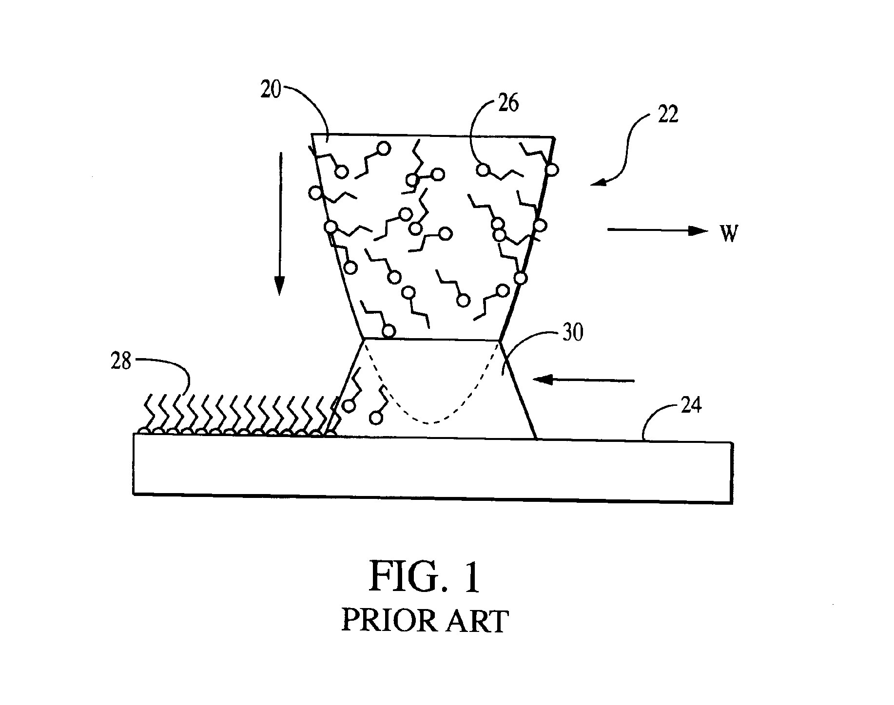
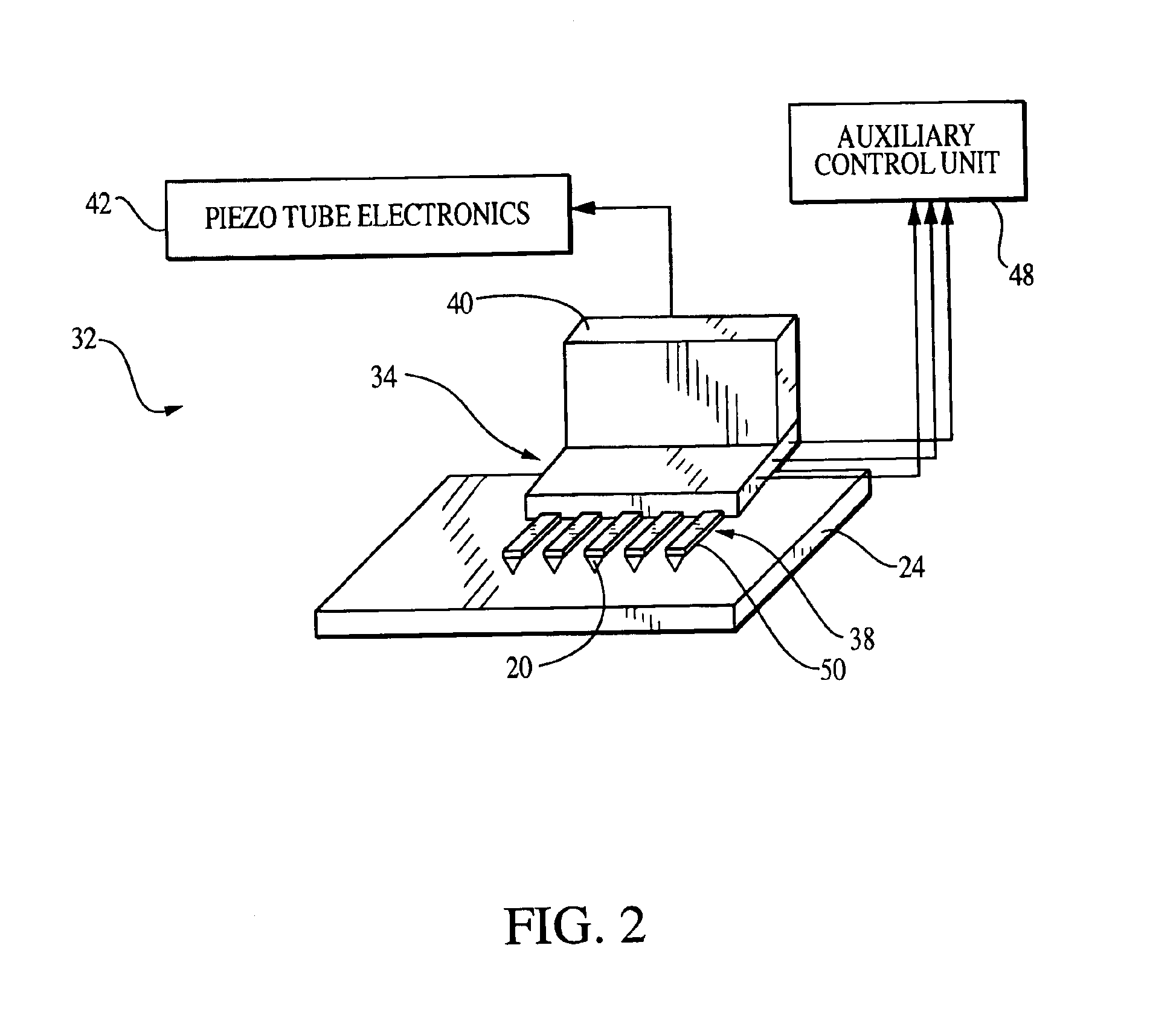
Generally speaking, the present invention provides active probes and active probe arrays, which are designed to achieve direct-write nanolithography, such as DPN. Devices according to the present invention can generate sub-100 nm patterns in a high speed, parallel, and controllable fashion. The active probe arrays offer greater functionality by allowing actuation of individual probes through supplying current or voltage to an actuator of the probe. The present invention is primarily directed to methods and devices for parallel DPN using active probe arrays, and methods for fabricating active probes and active probe arrays.

The active probe array can also be used for other existing or future surface patterning and lithography methods based on the scanning probe microscope (SPM) instrument family. An atomic force microscope (AFM) is considered a member of the SPM instrument family. Examples of such lithography systems include local thermal oxidation and displacement lithography.
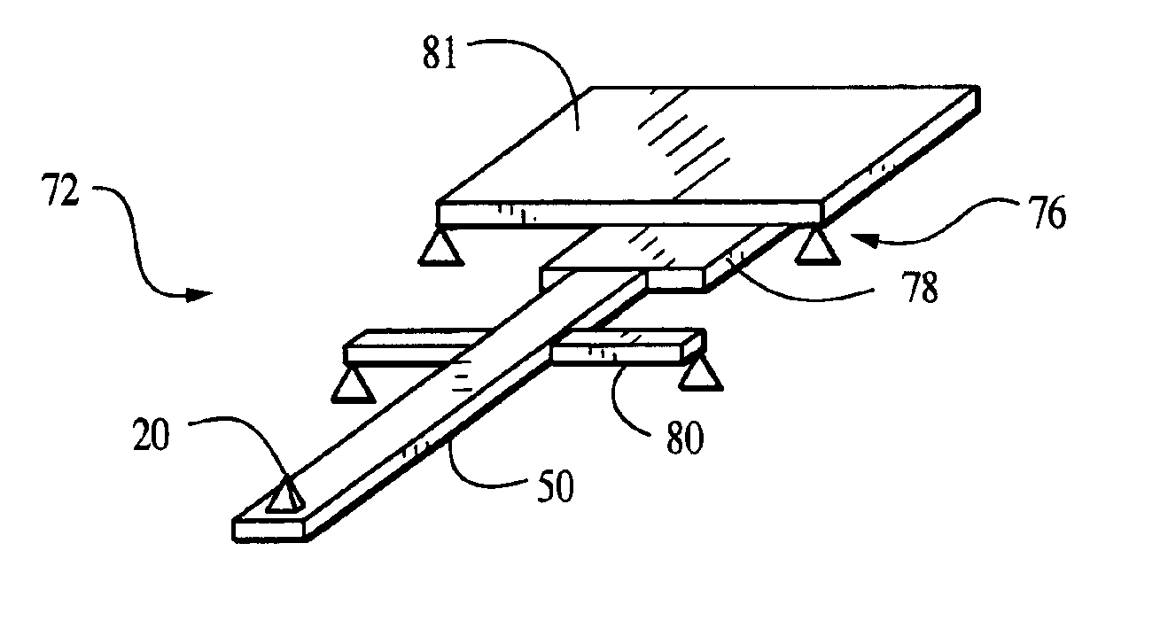
Referri...


PUM


Abstract

A microfabricated probe array for nanolithography and process for designing and fabricating the probe array. The probe array consists of individual probes that can be moved independently using thermal bimetallic actuation or electrostatic actuation methods. The probe array can be used to produce traces of diffusively transferred chemicals on the substrate with sub-1 micrometer resolution, and can function as an arrayed scanning probe microscope for subsequent reading and variation of transferred patterns.

Description

FIELD OF THE INVENTIONThe present invention relates generally to the art of efficient and high-speed generation of fine surface patterns made of chemical resist or biological substances using micromachined or microfabricated probes.BACKGROUND OF THE INVENTIONHigh-throughput lithography and surface patterning with extremely fine linewidths (e.g., on the order of 10-100 nm) are very important for the future growth of the microelectronics industry and nanotechnology. Next-generation integrated circuit technology will inevitably call for efficient and low-cost generation of features with a sub-100-nm linewidth. The emerging field of nanotechnology also requires patterning and functionalization of surfaces with a spatial resolution that is comparable with the scale of the molecules and cells that need to be manipulated and modified.The resolution of conventional projection optical lithographic systems, still the most widely used in the microelectronics industry, is limited by optical dif...

Claims


Application Information

Patent Timeline
IPC IPC(8): G03F7/20G03F7/00G12B21/02G12B21/00G01N35/10B81B3/00B81B7/04G01Q60/38G01Q70/16G01Q70/18G01Q80/00H01L21/027
CPCB82Y10/00B82Y40/00G01R1/073G03F7/0002G01N2035/1037Y10S977/874Y10S977/857G01Q80/00H01L21/20B82Y35/00
Inventor LIU, CHANGZHANG, MINGBULLEN, DAVID ANDREW
Owner THE BOARD OF TRUSTEES OF THE UNIV OF ILLINOIS
Why Eureka
Try Eureka