Semiconductor device having high breakdown voltage without increased on resistance

a technology of semiconductors and transistors, applied in the direction of semiconductor devices, electrical equipment, transistors, etc., can solve the problems of reducing the area of the channel and enlarge the size of the devi

Inactive Publication Date: 2005-03-15
DENSO CORP
View PDF16 Cites 11 Cited by
  • Summary
  • Abstract
  • Description
  • Claims
  • Application Information

AI Technical Summary

Benefits of technology

The n+-type drain region has a location where opposed parts of an epitaxial growth layer meet, thus the gate electrode does not need to be positioned to avoid this location. Therefore, the breakdown voltage is maintained without increasing the ON resistance. In addition, the n−-type drift region is formed in the p-type base region, so the electric field concentration at the bottom corner of the p-type base region is reduced.

Problems solved by technology

However, this modification enlarges the size of the device and decreases the area of the channel.

Method used


Image

  • Semiconductor device having high breakdown voltage without increased on resistance
  • Semiconductor device having high breakdown voltage without increased on resistance
  • Semiconductor device having high breakdown voltage without increased on resistance

Examples


first embodiment

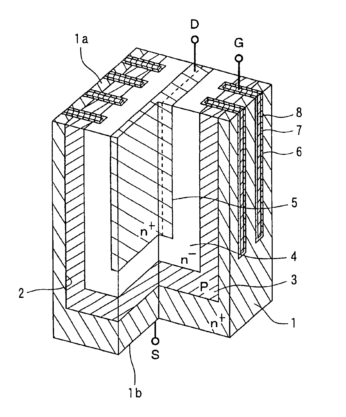
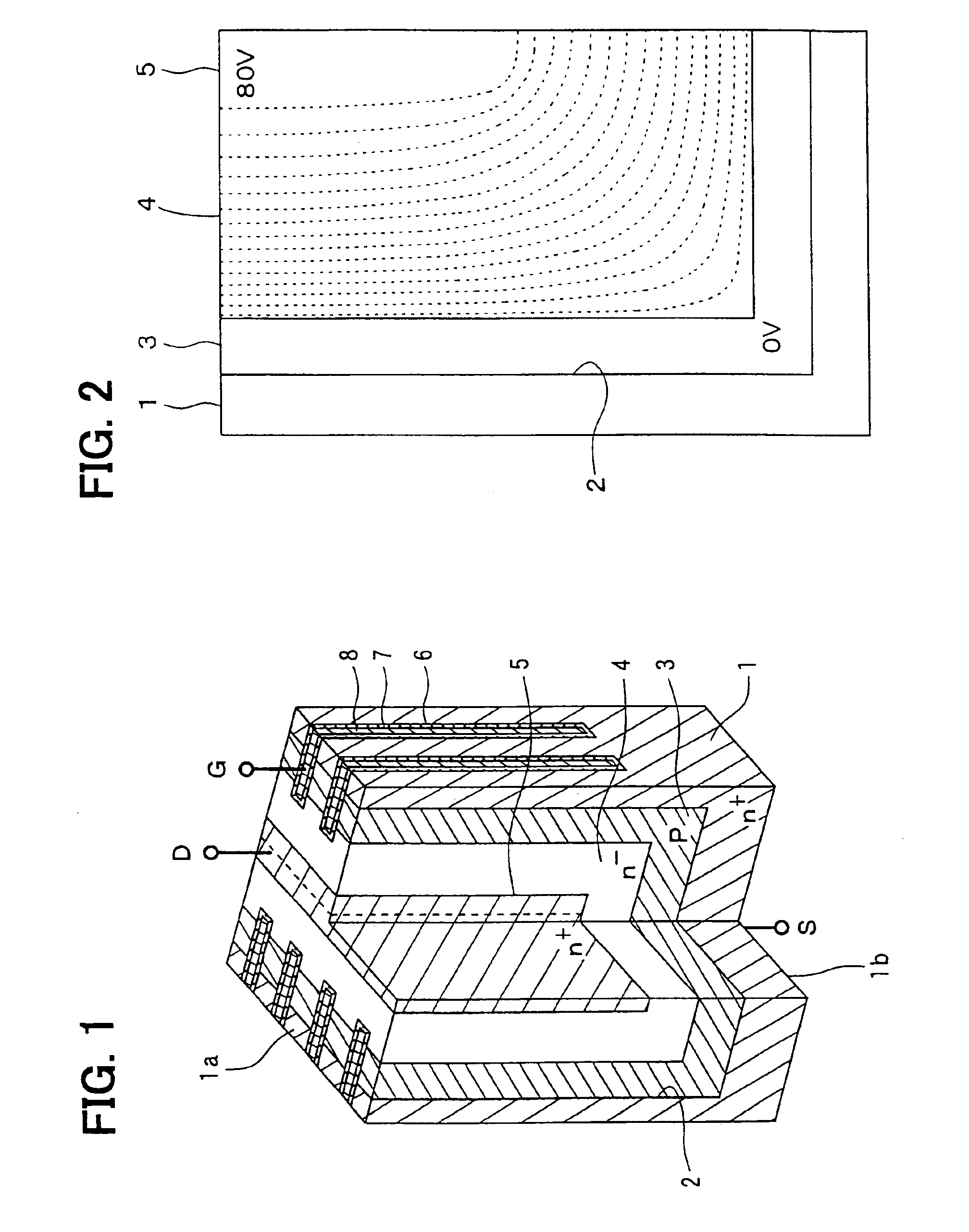
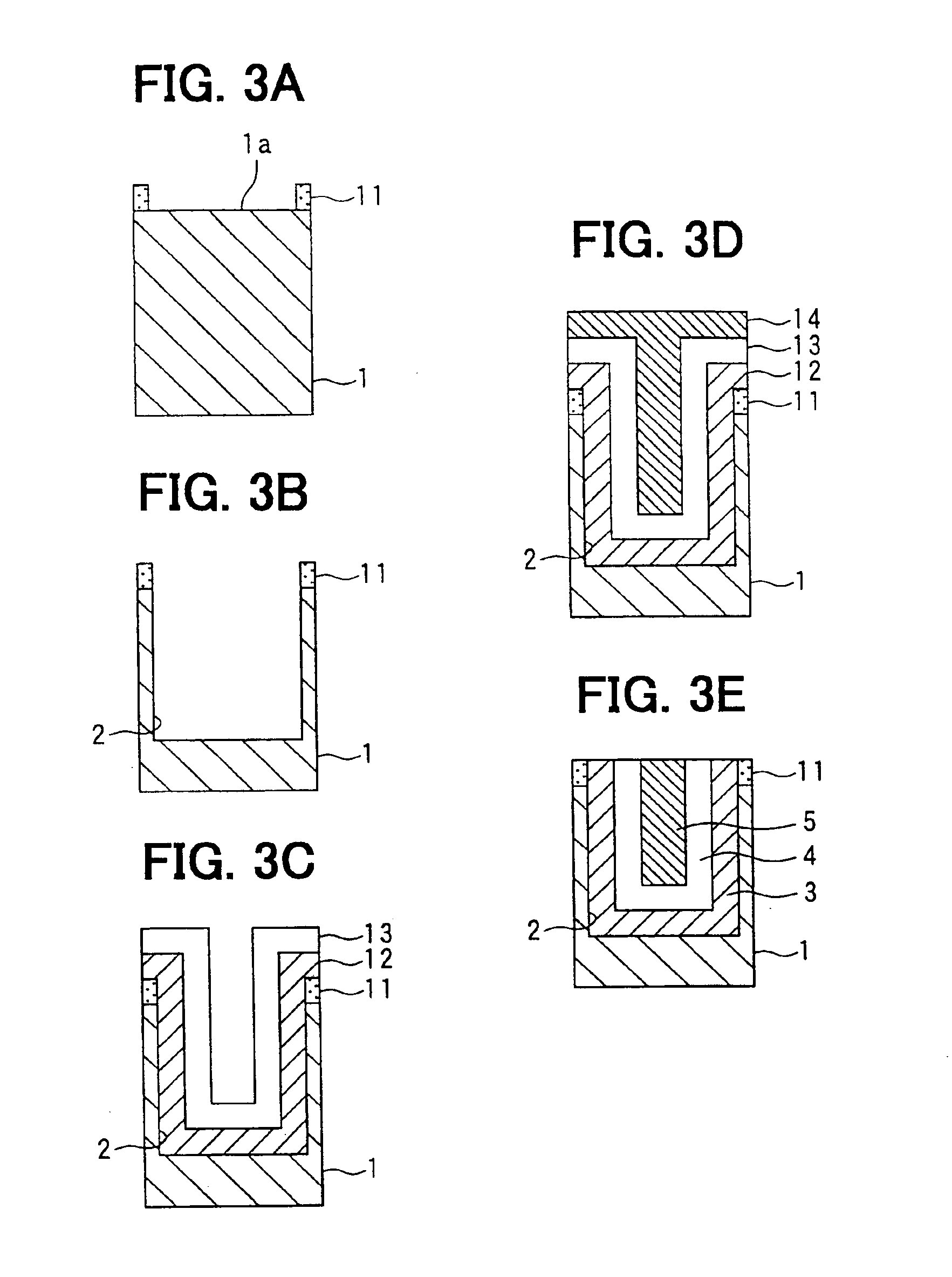
The structure of a power MOSFET in a first embodiment of the present invention will be described with reference to FIG. 1. In FIG. 1, the power MOSFET is fabricated from an n+-type substrate 1 having a top surface 1a, or main surface, and a back surface 1b, which is opposite to the top surface 1a. The substrate 1 forms an n+-type (first conduction type) source region that is homogeneously doped with any of phosphorus (P), arsenic (As), and antimony (Sb), which are n-type impurities, with a concentration ranging between 1×10¹⁸ and 1×1020 cm−3. A trench 2 (first trench) is formed in the substrate 1 with a predetermined depth from the top surface 1a. The depth ranges, for example, between 1 and 100 micrometers. A p-type (second conduction type) base region 3 having a thickness ranging between 0.1 and 5 micrometers is formed in the trench 2. The base region 3 is homogeneously doped with B (boron), which is a p-type impurity, with a concentration ranging between 1×10¹⁵ and 1×1018 cm−3. A...

second embodiment

As shown in FIG. 4, a power MOSFET according to a second embodiment includes an embedded metal layer 20, which electrically connects the n+-type source region 1 and the p-type base region 3 to apply the same potential to the n+-type source region 1 and the p-type base region 3. In the power MOSFET according to the first embodiment, the n+-type source region 1 and the p-type base region 3 are electrically connected using a metal wiring 25, as shown in FIG. 5. To connect the n+-type source region 1 and the p-type base region 3, a plurality of contact holes are formed in the interlayer insulating film and the metal wiring 25 is located in the contact hole. Therefore, the layout of the drain electrode is limited by the wiring 25. However, according to the second embodiment, this limitation is avoided by forming the metal layer 20.

third embodiment

As shown in FIG. 6, a power MOSFET according to a third embodiment includes a first embedded metal layer 20, the depth of which is close to that of the drain region 5, and a second embedded metal layer 21 located in the drain region 5. The depth of the second embedded metal layer 21 is close to that of the first embedded metal layer 20. With this structure, the resistances of the n+-type source region 1 and the drain region 5 are reduced. The power MOSFET in this embodiment is manufactured by forming a plurality of trenches extending from the top surface 1a at a boundary between the n+-type source region 1 and the p-type base region 3 and in the region 5 after the process shown in FIG. 3E. Then, the trenches are filled with the metal layers 20 and 21.


PUM


Abstract

A first trench is formed in a surface of an n+-type semiconductor substrate that forms a source region. A p-type base region, an n-type drift region, and an n+-type drain region are deposited in this order in the first trench using epitaxial growth. A second trench extending from the source region to the drift region through the base region is formed in the surface. A gate insulating film and a gate electrode are formed on a surface defining the second trench. The n+-type drain region has a location where growing surfaces come together in epitaxial growth and where a defect is likely to occur, and the gate electrode lacks such a location and thus avoids an increase in normalized ON resistance. Therefore, the breakdown voltage remains high without increasing the ON resistance.

Description

BACKGROUND OF THE INVENTIONThe present invention relates to a semiconductor device having an insulated gate. The present invention is applicable to a power MOSFET (Metal-Oxide-Silicon Field Effect Transistor), an IGBT (Insulated Gate Bipolar Transistor), or a thyristor.A power MOSFET having low ON-resistance was previously proposed by the present inventor. As shown in FIG. 14, the power MOSFET is has an n+-type substrate J1 making up an n+-type drain region and, an n−-type drift region J5, a p-type base layer J4, an n+-type source layer J3, and a plurality of gate electrodes J2. The gate electrodes J2 are plate-like and are embedded upright in the power MOSFET to divide the p-type base layer J4 and the n+-type source layer J3 into a plurality of p-type base regions J4 and a plurality of n+-type source regions J3, respectively. With this structure, channels are formed to extend in the lateral direction of FIG. 14.The power MOSFET shows especially low ON resistance in the range betwee...

Claims


Application Information

Patent Timeline
Patent Type & Authority Patents(United States)
IPC IPC(8): H01L29/66H01L29/78H01L29/423H01L29/40H01L29/749H01L29/06
CPCH01L29/0634H01L29/7801H01L29/4232H01L29/7831H01L29/4238H01L29/4175H01L29/7825H01L29/781
Inventor SAKAKIBARA, JUN
Owner DENSO CORP
Why Eureka
Try Eureka