Semiconductor device using an SOI substrate and having a trench isolation and method for fabricating the same

a technology of soi substrate and semiconductor device, which is applied in the direction of semiconductor device, electrical apparatus, transistor, etc., can solve the problems of crystal defects, low breakdown strength of device, increased dielectric breakdown strength, etc., and achieves the effect of suppressing stress generation and increasing dielectric breakdown strength

Inactive Publication Date: 2005-03-15
PANASONIC CORP
View PDF25 Cites 5 Cited by
  • Summary
  • Abstract
  • Description
  • Claims
  • Application Information

AI Technical Summary

Benefits of technology

It is therefore an object of the present invention is to increase the dielectric breakdown strength by relaxing the concentration of applied voltage in insulating films formed on the sides of a trench, while suppressing the generation of stress in active regions, in a semiconductor device using an SOI substrate and having a trench isolation.

Problems solved by technology

However, if a high voltage is applied between active regions at both sides of the isolation region in the known semiconductor device disclosed in the above publication, the high voltage is intensively applied to the thermal oxide films (thermal oxide films) in the isolation region, so that the device exhibits low breakdown strength.
On the other hand, if the thermal oxide films are made thick enough, the dielectric breakdown strength increases, but crystal defects occur in semiconductor crystal in the active regions.
These crystal defects occur because when the thick thermal oxide films are formed in a thermal oxidation process performed for a long time, the volume of the thermal oxide films increases so that the active regions undergo a large stress.
The occurrence of the crystal defects might deteriorate the current-driving capability of the transistors.

Method used


Image

  • Semiconductor device using an SOI substrate and having a trench isolation and method for fabricating the same
  • Semiconductor device using an SOI substrate and having a trench isolation and method for fabricating the same
  • Semiconductor device using an SOI substrate and having a trench isolation and method for fabricating the same

Examples


embodiment 1

(Structure of Semiconductor Device)

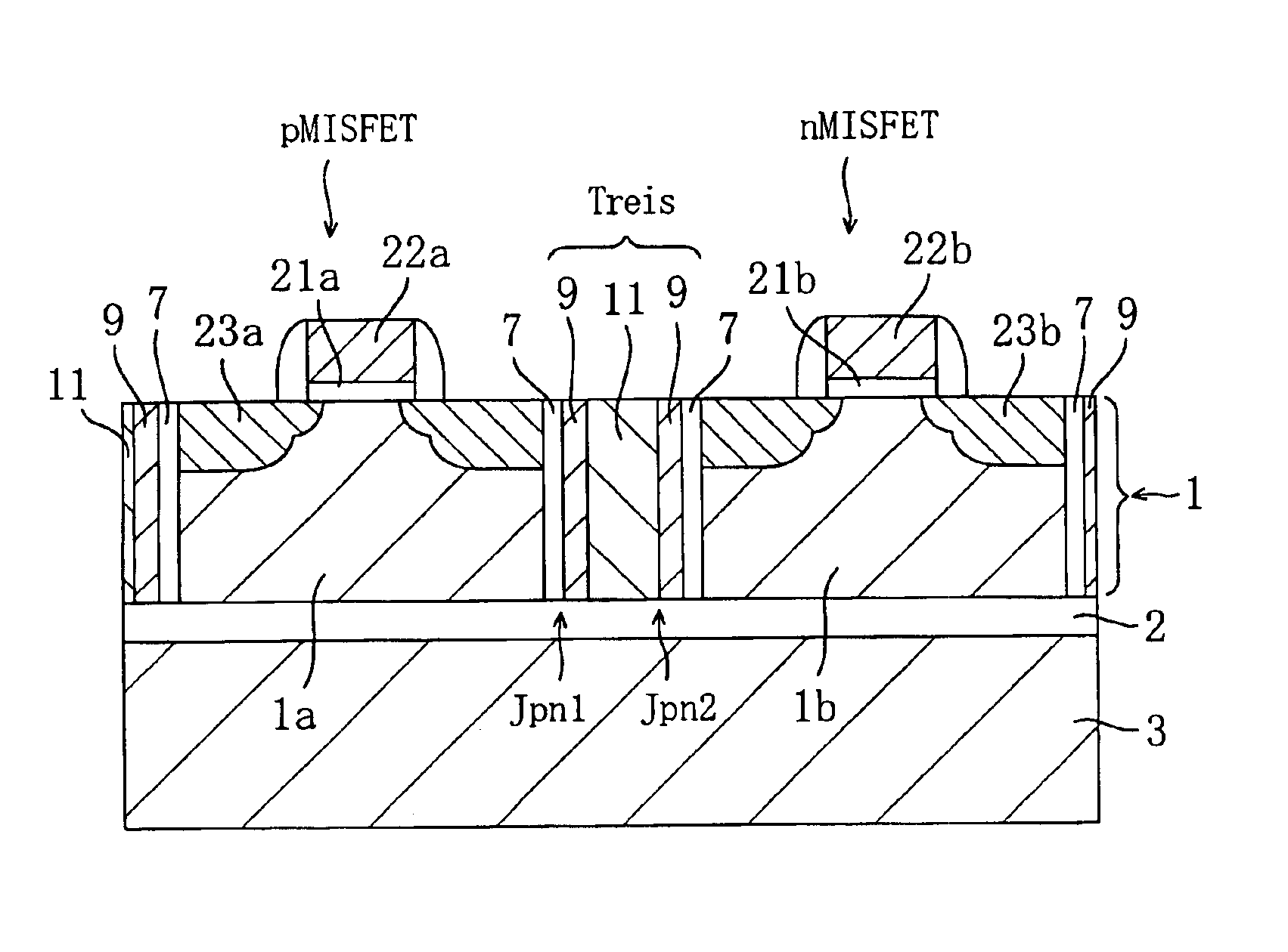
FIG. 1 is a cross-sectional view showing a structure of a semiconductor device using an SOI substrate according to a first embodiment of the present invention. As shown in FIG. 1, the semiconductor device of this embodiment is formed using an SOI substrate which includes: a semiconductor substrate 3 made of single-crystalline silicon; an insulating layer 2 with a thickness of 900 nm provided on the principal surface of the semiconductor substrate 3; and a semiconductor layer 1 with a thickness of 3.5 μm made of single-crystalline silicon and provided on the insulating layer 2.

The semiconductor layer 1 is divided into a large number of active regions 1a, 1b, . . . by a trench isolation region Treis. FIG. 1 shows only two of the active regions, i.e., the active regions 1a and 1b. A p-channel type MISFET (hereinafter, referred to as a pMISFET) is provided in the active region 1a, and an n-channel type MISFET (hereinafter, referred to as an nMISFET) is...

embodiment 2

In the method for fabricating a semiconductor device according to the first embodiment or the modified example of the first embodiment, part of the polycrystalline semiconductor layer 9 of the first conductivity type is changed into the polycrystalline semiconductor layer 11 of the second conductivity type using an ion implantation technique, in order to form the polycrystalline semiconductor layer 11. On the other hand, according to a method for fabricating a semiconductor device according to a second embodiment of the present invention, a process of forming a polycrystalline semiconductor layer of the second conductivity type with CVD including in-situ doping is adopted.

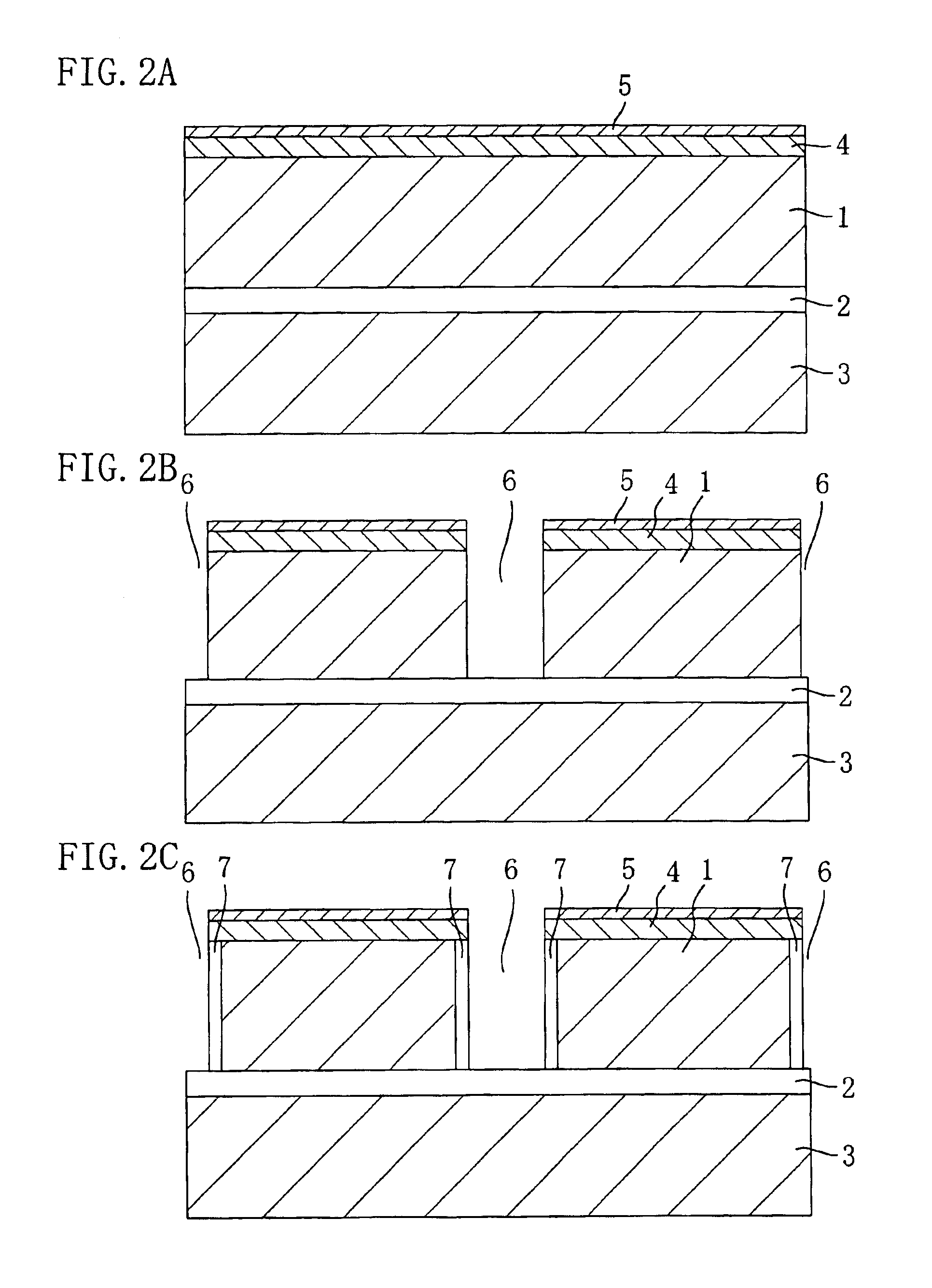
FIGS. 5A through 5C are cross-sectional views showing respective process steps for fabricating a semiconductor device of the second embodiment. In this embodiment, the process steps in the first embodiment or the modified example of the first embodiment shown in FIGS. 2A through 3B are performed before a process st...

embodiment 3

(Structure of Semiconductor Device)

FIG. 6 is a cross-sectional view showing a structure of a semiconductor device using an SOI substrate according to a third embodiment of the present invention. As shown in FIG. 6, the semiconductor device of this embodiment is formed using an SOI substrate including: a semiconductor substrate 3 of single-crystalline silicon; an insulating layer 2 with a thickness of 900 nm provided on the principal surface of the semiconductor substrate 3; and a semiconductor layer 1 with a thickness of 3.5 μm m made of single-crystalline silicon and provided on the insulating layer 2.

The semiconductor layer 1 is divided into a large number of active regions 1a, 1b, . . . by a trench isolation region Treis. FIG. 6 shows only two of the active regions, i.e., the active regions 1a and 1b. A pMISFET having the same structure as in the first embodiment is provided in the active region 1a, and an nMISFET having the same structure as in the first embodiment is provided i...


PUM


Abstract

A trench isolation region separating active regions in which MISFETs are formed includes: side insulating films covering the sides of a trench; polycrystalline semiconductor layers of a first conductivity type covering the respective sides of the side insulating films; and a polycrystalline semiconductor layer of a second conductivity type filling a gap between the polycrystalline semiconductor layers of the first conductivity type. Two pn junctions extending along the depth direction of the trench are formed between each of the polycrystalline semiconductor layers of the first conductivity type and the polycrystalline semiconductor layer of the second conductivity type. Upon application of a voltage between the active regions, a depletion layer expands in one of the pn junctions, so that the voltage is also partly applied to the depletion layer. As a result, the concentration of electric field in the side insulating films is relaxed.

Description

BACKGROUND OF THE INVENTIONWith the recent reduction in size of semiconductor elements such as transistors, trench isolation has been adopted as a technique for isolating transistors in semiconductor integrated circuits. Specifically, this trench isolation is a technique for isolating adjacent active regions by forming a trench (groove) in a surface region of a semiconductor substrate to define the active regions and then filling the trench with an insulator film.In particular, in a semiconductor device using a silicon on insulator (SOI) substrate with a structure in which a semiconductor layer for forming active regions therein is provided on an insulating layer, if a trench is formed to reach the insulating layer, isolation can be made as intended. For example, in Japanese Laid-Open Publication No. 61-059852, a trench is formed in a semiconductor layer to reach an insulating layer, using an SOI substrate formed by a bonding technique, thermal oxide films (side insulating films) ar...

Claims


Application Information

Patent Timeline
Patent Type & Authority Patents(United States)
IPC IPC(8): H01L21/70H01L21/762H01L27/12H01L21/84
CPCH01L21/76264H01L21/76275H01L27/1203H01L21/84H01L21/76283H01L21/76286
Inventor NAKAZAWA, SATOSHIOUCHI, SATORUUEMOTO, YASUHIRO
Owner PANASONIC CORP
Why Eureka
Try Eureka