
Semiconductor integrated circuit device

a technology of integrated circuit and semiconductor, applied in the direction of generating/distributing signals, pulse techniques, instruments, etc., can solve the problems of more delay of clock signals, affecting the efficiency of vlsis, and unable to consider the optimal arrangement of skew reduction for vlsis, so as to minimize clock skew

Inactive Publication Date: 2005-03-15
RENESAS ELECTRONICS CORP
View PDF18 Cites 4 Cited by
  • Summary
  • Abstract
  • Description
  • Claims
  • Application Information

AI Technical Summary

Benefits of technology

It is therefore an object of the present invention to provide a semiconductor integrated circuit device having a clock skew-lowering layout that ensures reduced wiring delays, enhanced packaging density and low clock power dissipation.
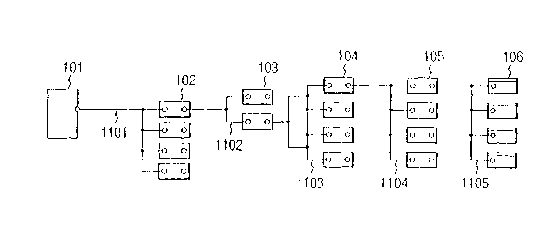
The lower the stage, the greater the number of clock drivers furnished. In that structure, clock lines connecting lower stage clock drivers are made to have not equal lengths but the shortest possible lengths. The arrangement shortens the overall clock wiring, reduces wiring delays, enhances packaging density, and lowers clock power dissipation. Since the lower stage clock drivers are connected by lines that are shorter than those connecting the upper stage clock drivers, the lower stage clock drivers may have the shortest possible wiring entailing negligible clock skew. Because the upper stage clock drivers are connected by extended wiring, the lines constituting such wiring are made to be equal in length in order to minimize clock skew.
The clock logic circuits control the supply of clock signals to individual function blocks corresponding to the intermediate clock drivers in question. The setup implements a clock signal supply scheme suitable for a VLSI while minimizing clock skew. Preferably, next-to-last stage clock drivers may have clock logic circuits for supply of clock signals to the flip-flops of random logic circuits and input / output pads, and both last stage and next-to-last stage clock drivers may have clock logic circuits for the supply of clock signals to the flip-flops of data paths.

Problems solved by technology

The conventional techniques outlined above have failed to consider optimum arrangements of skew reduction for VLSIs.
The resulting disadvantages include more delays of clock signals and higher power dissipation.
Furthermore, the conventional techniques above have disregarded an optimum clock layout for each of the functional portions or for each of a plurality of clock phases in connection with LSIs.
The conventional techniques have so far shied away from providing any optimum clock layout for the diverse internal arrangements of the LSI.

Method used


Image

  • Semiconductor integrated circuit device
  • Semiconductor integrated circuit device
  • Semiconductor integrated circuit device

Examples


Embodiment Construction

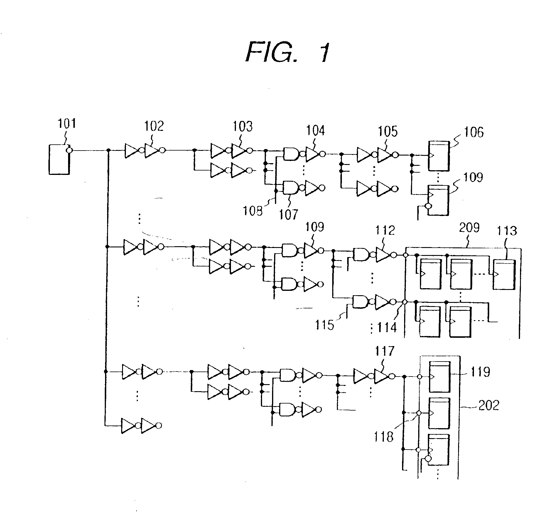
FIG. 1 is a schematic diagram showing clock logic circuits applicable to a semiconductor integrated circuit device embodying the invention. This embodiment comprises four stages of clock drivers through which a clock signal generator 101 supplies clock signals to all flip-flops 106 inside the chip. The flip-flops are located in random logic circuits, data paths, and input / output pads.

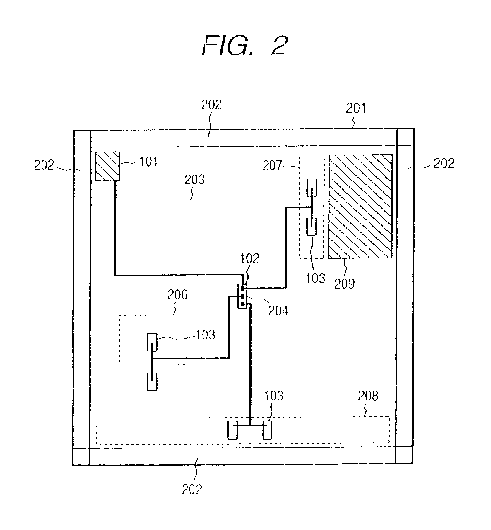
The clock drivers at each stage play the roles described below. Clock drivers 102, situated at the first stage as viewed from the clock signal generator, are called root clock drivers. These drivers distribute throughout the entire chip the clock signals output by the clock signal generator.

Second stage clock drivers 103 distribute clock signals to third stage clock drivers 104. The drivers 104 are located in regions each made up of a number of logic blocks in the chip.

The third stage clock drivers 104 and fourth stage clock drivers 105 serve to distribute clock signals to all flip-flops in the logic bl...


PUM


Abstract

A semiconductor integrated circuit device for minimizing clock skew over clock wiring shortened for reduced wiring delays. A plurality of stages of clock drivers are provided on clock wiring paths ranging from a clock generator to flip-flops. Clock lines connecting upper stage clock drivers are equalized in length in the form of a tree structure, and clock lines connecting lower stage clock drivers are made as short as possible.

Description

BACKGROUND OF THE INVENTIONThe present invention relates to a semiconductor integrated circuit device and, more particularly, to a semiconductor integrated circuit device having clock wiring with reduced clock skew.Some semiconductor integrated circuit devices, such as VLSIs, include a synchronous circuit having flip-flops driven by a common clock signal. To make such a synchronous circuit operate more rapidly, these semiconductor integrated circuit devices require that clock skew (i.e., differences in clock supply timing between flip-flops) be minimized for removal of signal-to-signal timing differences.Various layout design techniques for reducing such clock skew have been proposed. One such technique involves installing tree-structure paths between a clock signal generator and a plurality of flip-flops, wherein the length of the path between the generator and each flip-flop is suitably adjusted. Another technique, which is disclosed in Japanese Published Unexamined Patent Applica...

Claims


Application Information

Patent Timeline
IPC IPC(8): G06F1/10H03L7/00H01L21/822H01L27/04
CPCG06F1/10H03L7/00H01L27/10
Inventor NITTA, YUSUKEHATTORI, TOSHIHIRO
Owner RENESAS ELECTRONICS CORP
Learn More