Optical waveguide and their application of the optical communication system

a technology of optical communication system and optical waveguide, which is applied in the direction of instruments, cladded optical fibres, optical elements, etc., can solve the problems of excessive complex process steps to incur higher fabrication costs, and excess insertion loss in the path of reflected light, etc., to achieve excellent characteristics, high fabrication tolerance, and optical system

Inactive Publication Date: 2005-03-15
HITACHI LTD +1
View PDF15 Cites 8 Cited by
  • Summary
  • Abstract
  • Description
  • Claims
  • Application Information

AI Technical Summary

Benefits of technology

It is therefore an object of the present invention to provide an optical module structure with high fabrication tolerance and with excellent characteristics and an optical system using the same.
Another object of the present invention is to provide an optical module structure that can be scaled down without impairing the characteristic of dicing tolerance and an optical system using the same.
By thus forming the optical waveguide for guiding reflected light with a core which is substantially not less than twice as large as the core of the other optical waveguide, the reflected light from the filter is more likely to be incident upon the core so that, even if the wavelength selection filter is displaced and axial displacement occurs in the path, the occurrence of an excess loss is suppressed. For example, the displacement tolerance on the filter in a direction horizontal to the substrate surface can be increased if the width of the core is increased and the displacement tolerance on the filter in a direction perpendicular to the substrate surface can be increased if the thickness of the core is increased. It will easily be appreciated that an optical waveguide with a core having both an increased width and an increased thickness may also be used appropriately.

Problems solved by technology

However, the following problems are likely to occur when the foregoing conventional embodiments are put into practical use.
The present structure also has the problem that the displacement of the wavelength selection filter 4 causes an excess insertion loss in the path of reflected light.
In this case, however, the process steps are complicated to incur higher fabrication cost.
However, the structure shown in FIG. 19 is similar to the structure shown in FIG. 18 in that an excess insertion loss is likely to occur in the path of the reflected light due to the displacement of the filter.
However, the step of performing oblique dicing with respect to the surface is more complicated than the step of perpendicular dicing so that mounting cost is likely to be increased.
However, a complicated mounting process is required to place the wavelength selection filter, the filter for cutting the light for transmission, and the photodiode in succession on the surface of the optical waveguide so that a higher cost for the module is incurred.
However, such a device is special and less available so that it presents an obstacle when the optical transmitter / receiver module is mass produced at low cost as a general-purpose product.
Thus, it has been difficult to fabricate an optical module with excellent characteristics at low cost even with the foregoing prior art technologies.

Method used


Image

  • Optical waveguide and their application of the optical communication system
  • Optical waveguide and their application of the optical communication system
  • Optical waveguide and their application of the optical communication system

Examples


first embodiment

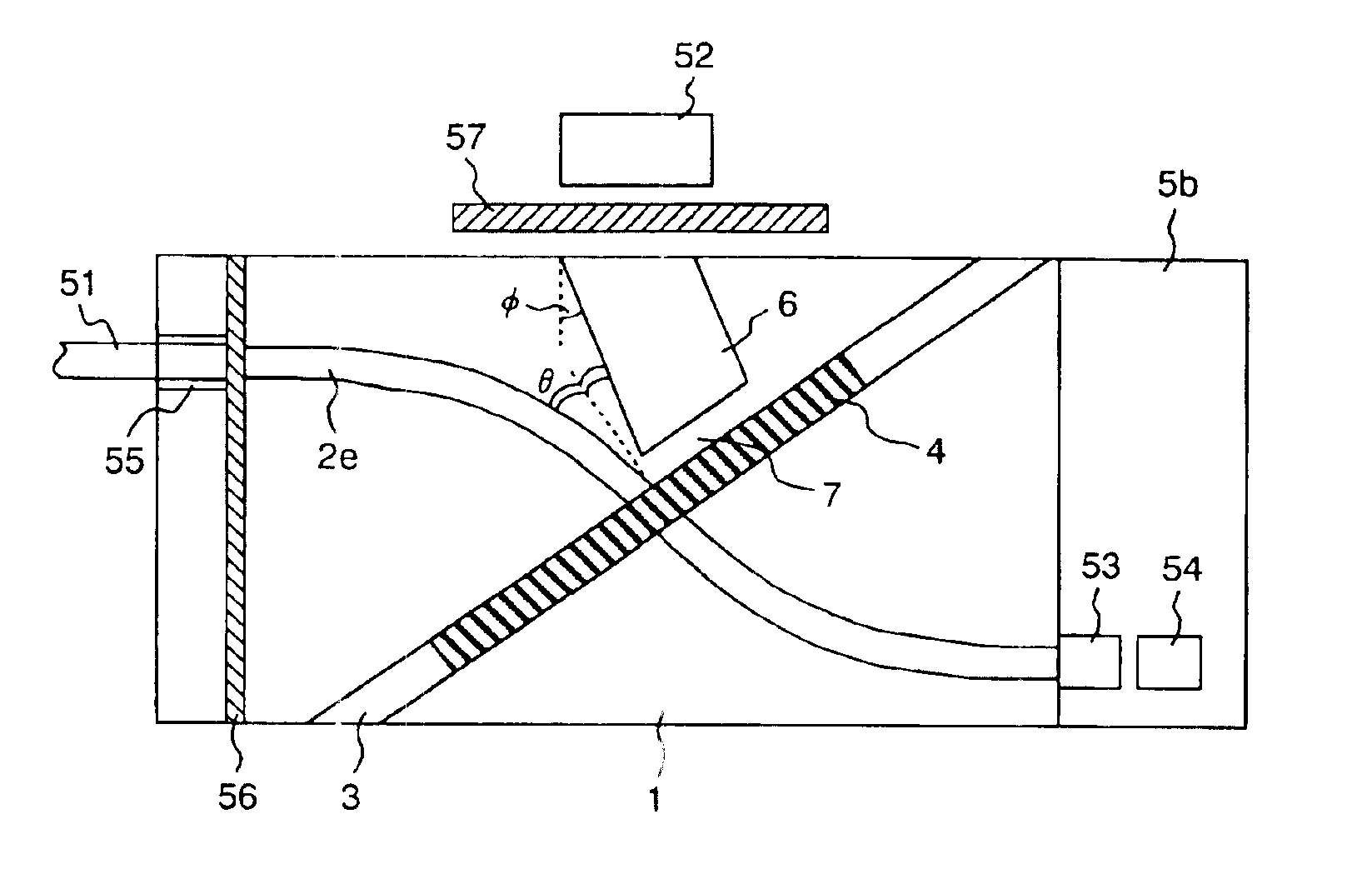
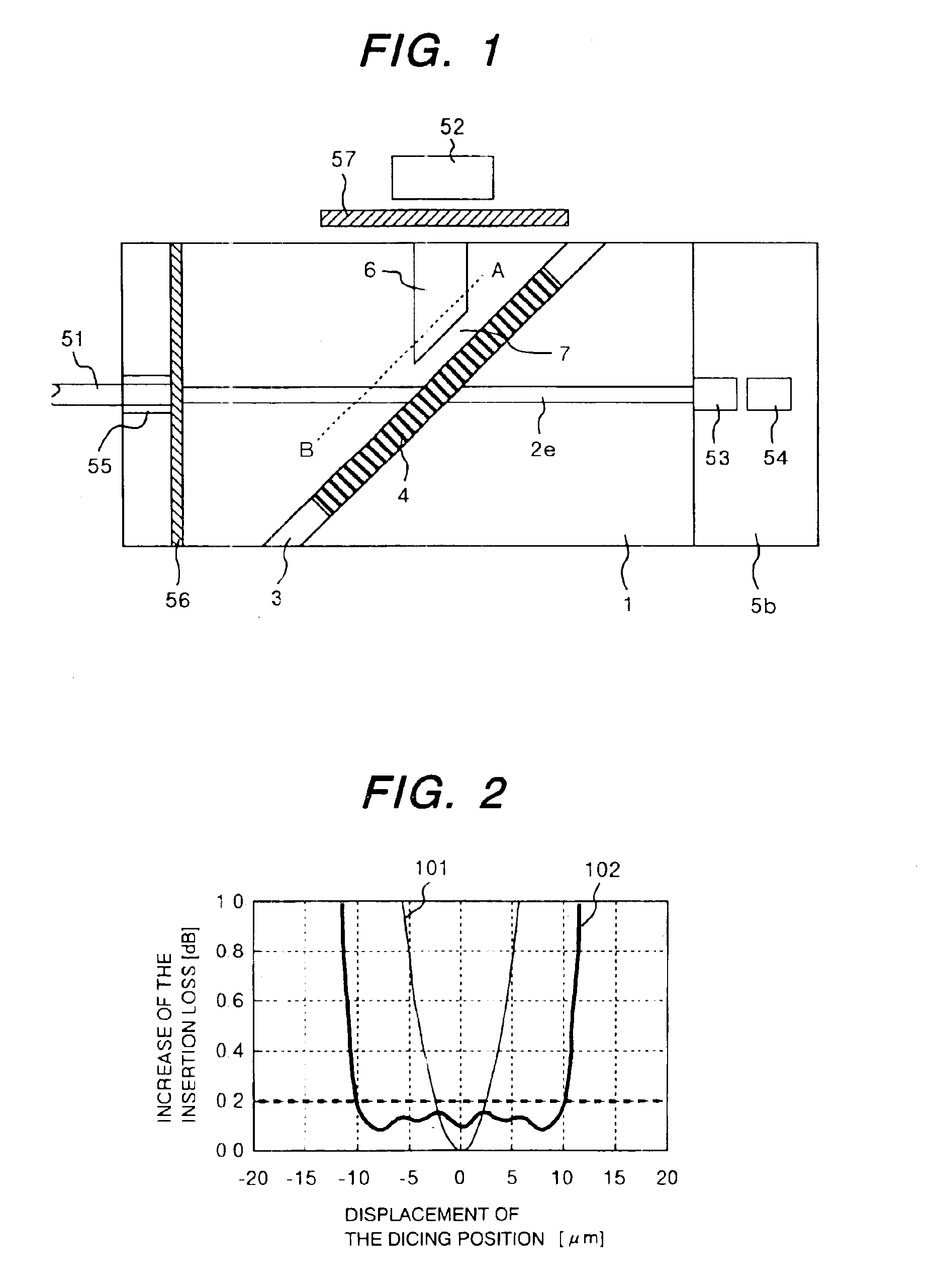
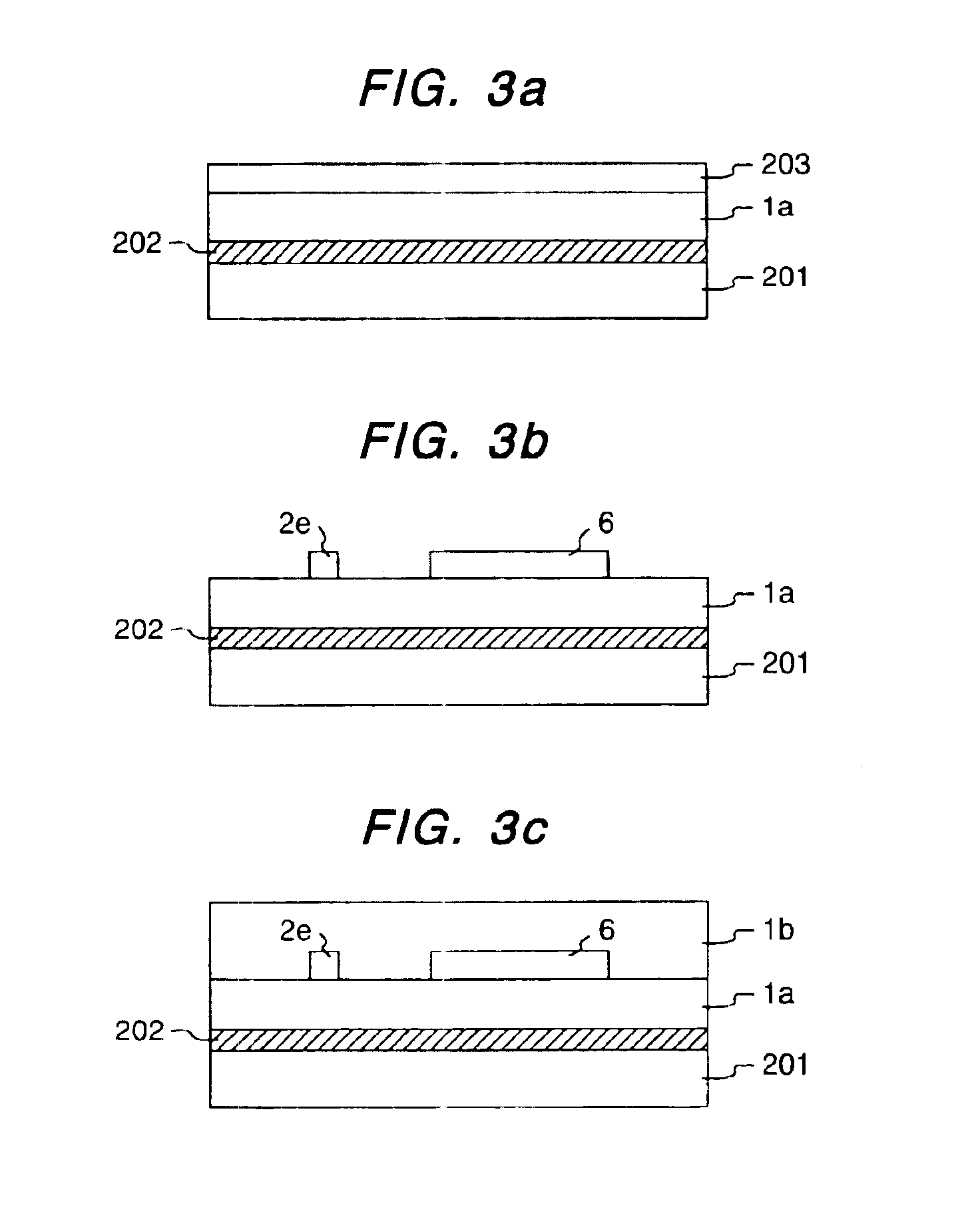
FIG. 1 is a generally plan view showing an optical transmitter / receiver module of wavelength division multiplexing type having an optical waveguide according to the present invention. The module according to the present embodiment has a linear single-mode optical waveguide (first optical waveguide) 2e provided in a substrate (clad) 1 and a multi-mode optical waveguide (second optical waveguide) 6 branched from the first optical waveguide 2e in the vicinity of a dicing trench 3. A gap 7 is provided between the first and second optical waveguides 2e and 6 to prevent the occurrence of air bubbles during fabrication. The wavelength selection filter 4 is disposed in the dicing trench 3.

In the optical transmitter / receiver module of wavelength division multiplexing type according to the present embodiment, a light signal with a wavelength λ2 from a semiconductor laser 53 mounted on the device mounting portion 5b formed in the same single substrate as the optical waveguides is incident on t...

second embodiment

FIG. 4 shows the present invention. In an optical transmitter / receiver module of wavelength division multiplexing type according to the present embodiment also, the size of the core of the optical waveguide 6 for guiding reflected light from the filter is substantially not less than twice and not more than twenty times as large as the size of the core of the first optical waveguide 2e. The present embodiment may also impart a level difference to the path of the first optical waveguide 2e anterior and posterior to the filter in correspondence with the refraction of light resulting from the refractive index difference between the optical waveguide layer and the filter. With the present structure, a loss in the direction of transmission due to the refraction of light by the filter can be reduced.

third embodiment

FIG. 5 shows the present invention. In the present module, the size of the core of the optical waveguide 6 for guiding reflected light from the filter is substantially not less than twice and not more than twenty times as large as the size of the core of the first optical waveguide 2e. In the case where the generation of air bubbles can be suppressed during the fabrication of the optical waveguides or where the influence of generated air bubbles is negligible, a gap need not be provided between the first and second optical waveguides 2e and 6 in the same manner as in the present embodiment.


PUM


Abstract

An optical transmitter / receiver module of wavelength division multiplexing type which undergoes a reduced excess loss resulting from the displacement of a dicing position is fabricated with a high yield rate. An optical waveguide for guiding reflected light from a wavelength selection filter has a core substantially larger in size than the core of each of the other optical waveguides.

Description

FIELD OF THE INVENTIONThe present invention relates to an optical transmitter / receiver module for wavelength division multiplexing communication, to a PLC (Planar Lightwave Circuit), and to an optical system using the same.BACKGROUND OF THE INVENTIONWavelength division multiplexing communication using an optical fiber is an important technology for transmitting a large amount of information at a high speed. In recent years, a vigorous attempt has been made to provide a smaller-size and lower-cost optical transmitter / receiver module for use in wavelength division multiplexing communication by using a PLC to compose the module.FIG. 18 is a conceptual view of a conventionally known optical module of PLC type, which is a cross-sectional view taken in a direction parallel to the surface of an optical waveguide substrate. Such an optical module is disclosed in “European Conference on Optical Communication p.629 (1998)” (Document 1). In the present module, a light signal with a wavelength ...

Claims


Application Information

Patent Timeline
Patent Type & Authority Patents(United States)
IPC IPC(8): G02B6/28G02B6/42G02B6/122
CPCG02B6/4246G02B6/2852
Inventor TAKAHASHI, MAKOTOIDO, TATEMISANO, HIROHISASHIBATA, TOMOAKI
Owner HITACHI LTD
Why Eureka
Try Eureka