

Patterning method with micro-contact printing and its printed product
a micro-contact printing and pattern technology, applied in the field of pattern printing of micro-contacts, can solve the problems of limited reproduction of micro-contact printed patterns in the mass-production of micro-contact printed, low heat resistance and mechanical resistance of photolithography, and the limit of micro-contact printed patterns of the order of hundreds m
- Summary
- Abstract
- Description
- Claims
- Application Information
AI Technical Summary
Benefits of technology
Problems solved by technology
Method used
Image

Examples
example 1
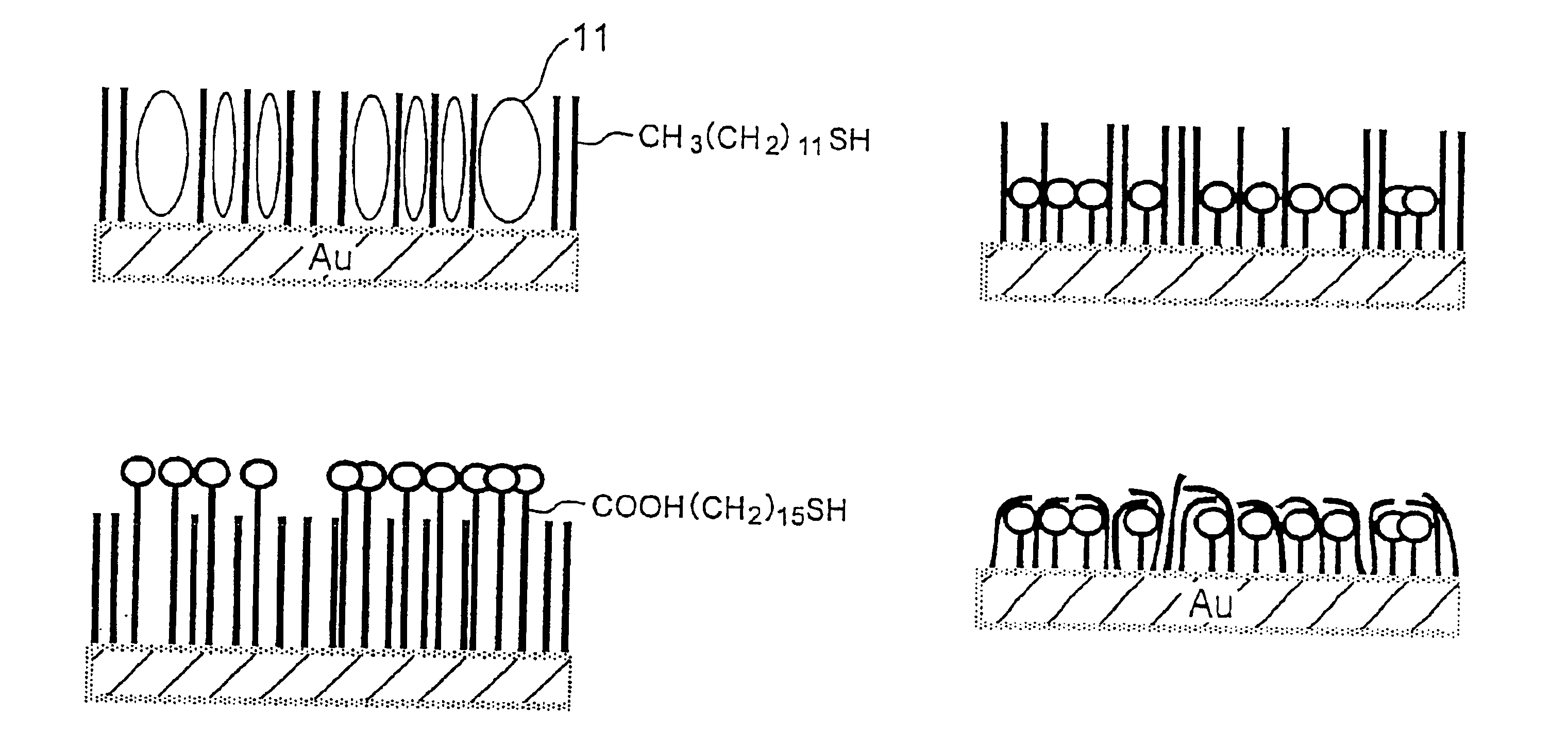
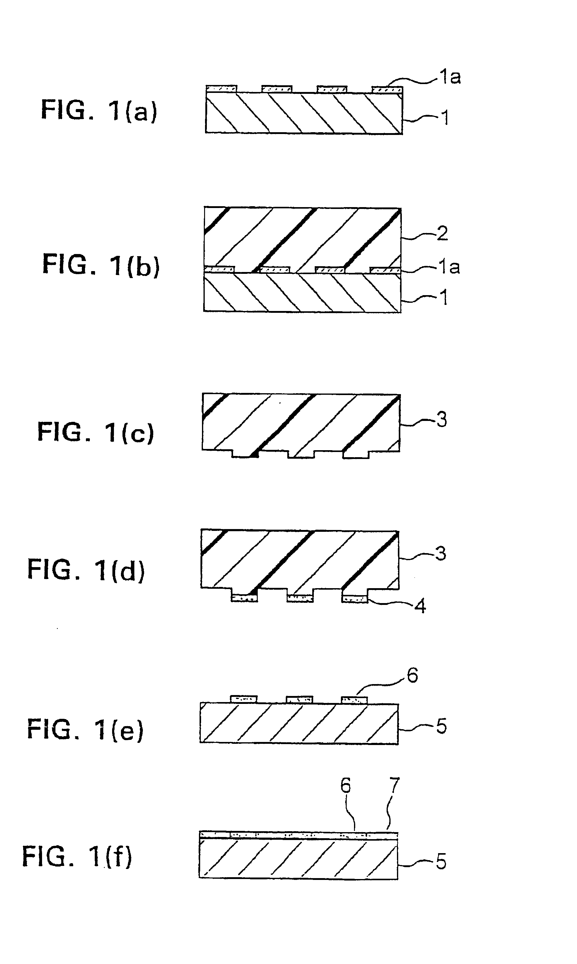
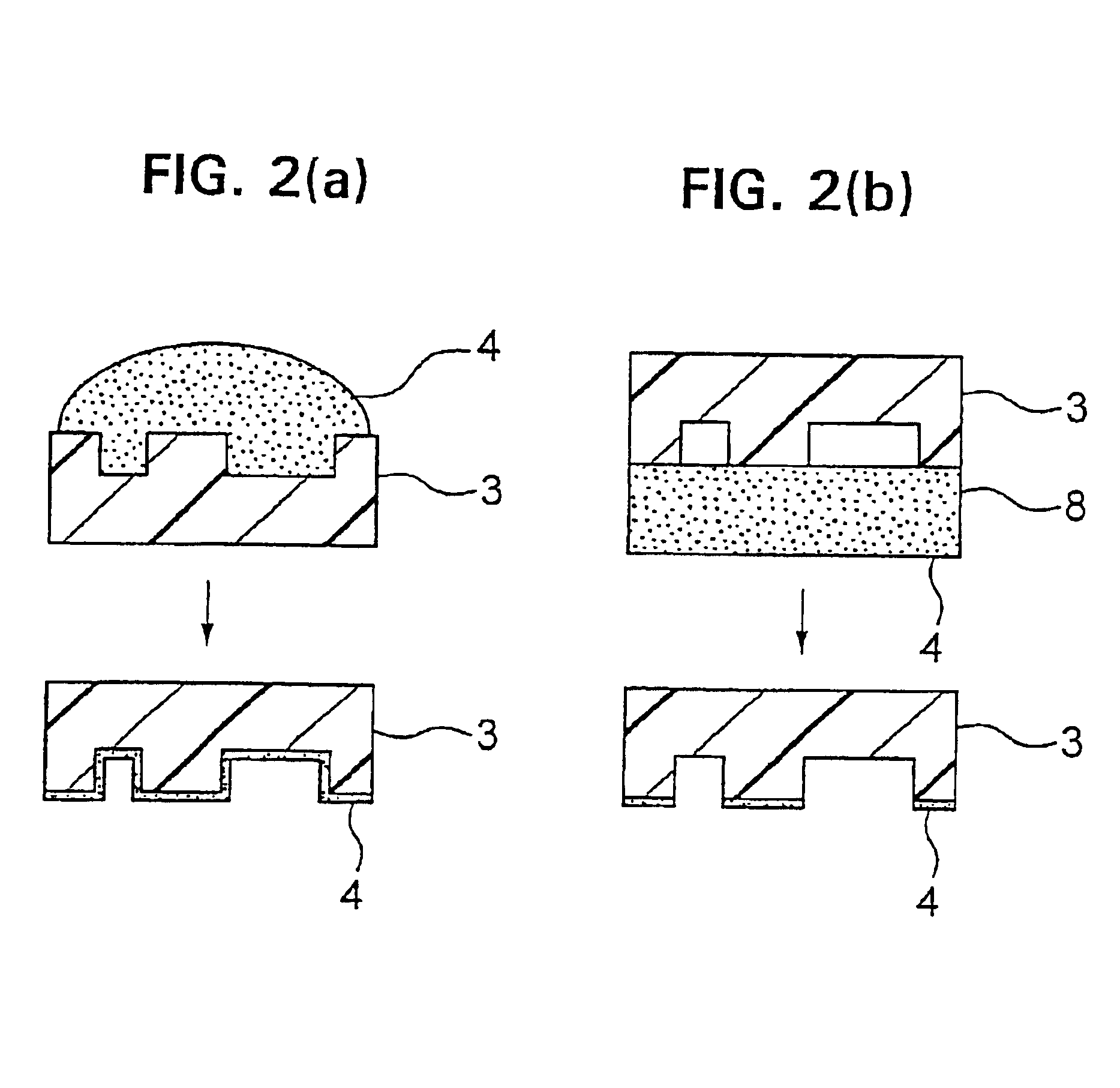
First, a thin film of chromium was formed on a surface of a quartz plate by a sputtering method. Resist patterns with a thickness of 4000 Å were formed on the quartz plate with a thin film of chromium to form a master with a height on the surface of the quartz plate with the thin film of chromium. PDMS resin was spin-coated or cast on the surface of the master with resist patterns and was heat-treated at 65° C. for four hours to be hardened. Thereafter, the hardened PDMS resin was removed from the master to form a stamp. Then, a molecular ink including an ethanol solution of CH3(CH2)19SH was applied on the stamp by the contact inking method.
On the other hand, a substrate with an evaporation layer of gold on a glass plate was provided. The stamp having the molecular ink on the surface thereof was pressed against the surface of the substrate by which the molecular ink was transferred to the substrate. Thereby, micro-contact printed patterns were formed.
Then, chemical modification was ...
example 2
First, a thin film of chromium was formed on a surface of a quartz plate by the sputtering method. Resist patterns with a thickness of 4000 Å were formed on the quartz plate with a thin film of chromium to form a master with a height on the surface of the quartz plate with the thin film of chromium. PDMS resin was spin-coated on the surface of the master with the resist patterns and was heat-treated at 65° C. for four hours to be hardened. Thereafter, the hardened PDMS resin was removed from the master to form a stamp. Then, a molecular ink including an ethanol solution of CH3(CH2)19SH was applied on the stamp by the contact inking method.
On the other hand, a substrate with an evaporation layer of gold on a glass plate was provided. The stamp having the molecular ink on the surface thereof was pressed against the surface of the substrate so that the molecular ink was transferred to the substrate. Thereby, micro-contact printed patterns were formed.
Then, the substrate with the micro-...
example 3
After forming the printed product according to the Example, chemical modification by hydrophobic molecules was again given to the micro-contact printed patterns using a stamp filled with hydrophobic ink. In the second process, parts of defects in the micro-contact printed patterns can be perfectly mended. Thereby, a printed product with a further higher contrast between the micro-contact printed patterns and the area of the surface of the substrate around the micro-contact printed patterns was formed.
PUM
| Property | Measurement | Unit |
|---|---|---|
| Area | aaaaa | aaaaa |
| Hydrophilicity | aaaaa | aaaaa |
| Hydrophobicity | aaaaa | aaaaa |
Abstract
Description
Claims
Application Information