Process and apparatus for treating a workpiece such as a semiconductor wafer

a technology of workpieces and processing equipment, applied in the direction of sustainable manufacturing/processing, final product manufacturing, cleaning using liquids, etc., can solve the problems of high performance degradation of devices, silicon dioxide, fabrication structure, and can be considered contaminants, so as to reduce contamination, speed up processing, and high clean level

Inactive Publication Date: 2005-03-22
OEM GRP LLC
View PDF86 Cites 59 Cited by
  • Summary
  • Abstract
  • Description
  • Claims
  • Application Information

AI Technical Summary

Benefits of technology

A novel chemistry, application technique, and system is used to reduce the contamination and speed up processing in the manufacturing of semiconductor wafers, memory disks, photomasks, optical media, and other substrates (collectively referred to here as “wafers”) requiring a high level of clean. Contamination may occur from organics, particles, metal / ions, and silicon dioxide. Cleaning of wafers is achieved by delivery of a chemical stream to the workpiece surface. Ozone is delivered either into the liquid process stream or into the process environment. The chemical stream, which may be in the form of a liquid or vapor, is applied to the wafer in a system which allows for control of the liquid boundary layer thickness. The chemical stream may include ammonium hydroxide for simultaneous particle and organic removal, another chemical to raise the pH of the solution, or other chemical additives designed to accomplish one or more specific cleaning steps.
4) The process utilizes a mixed effluent having a higher concentration of ozone in combination with a higher flow rate for increasing the rate at which fresh reactants are supplied to the surface of the wafer.

Problems solved by technology

This renders the devices highly susceptible to performance degradation due to organic, particulates or metallic / ionic contamination.
Even silicon dioxide, which is used in the fabrication structure, can be considered a contaminant if the quality or thickness of the oxide does not meet design parameters.
Although this portion of the process does an outstanding job of removing particles by simultaneously growing and etching away a silicon dioxide film on the surface of a bare silicon wafer (in conjunction with creating a zeta potential which favors particle removal), it has the drawback of causing metals, such as iron and aluminum, in solution to deposit on the silicon surface.
In recent years, thin oxides have been cause for concern in device performance, so “hydrochloric acid last” chemistries have been developed.
Although the four-chemistry clean process described above has been effective for a number of years, it nevertheless has certain deficiencies.
Such deficiencies include the high cost of chemicals, the lengthy process time required to get wafers through the various cleaning steps, high consumption of water due to the need for extensive rinsing between chemical steps, and high disposal costs.
However, such cleaning processes have failed to fully address all of the major cleaning concerns of the semiconductor processing industry.
More particularly, they have failed to fully address the problem of minimizing contamination from one or more of the following contaminants: organics, particles, metals / ions, and silicon dioxide.

Method used


Image

  • Process and apparatus for treating a workpiece such as a semiconductor wafer
  • Process and apparatus for treating a workpiece such as a semiconductor wafer
  • Process and apparatus for treating a workpiece such as a semiconductor wafer

Examples


Embodiment Construction

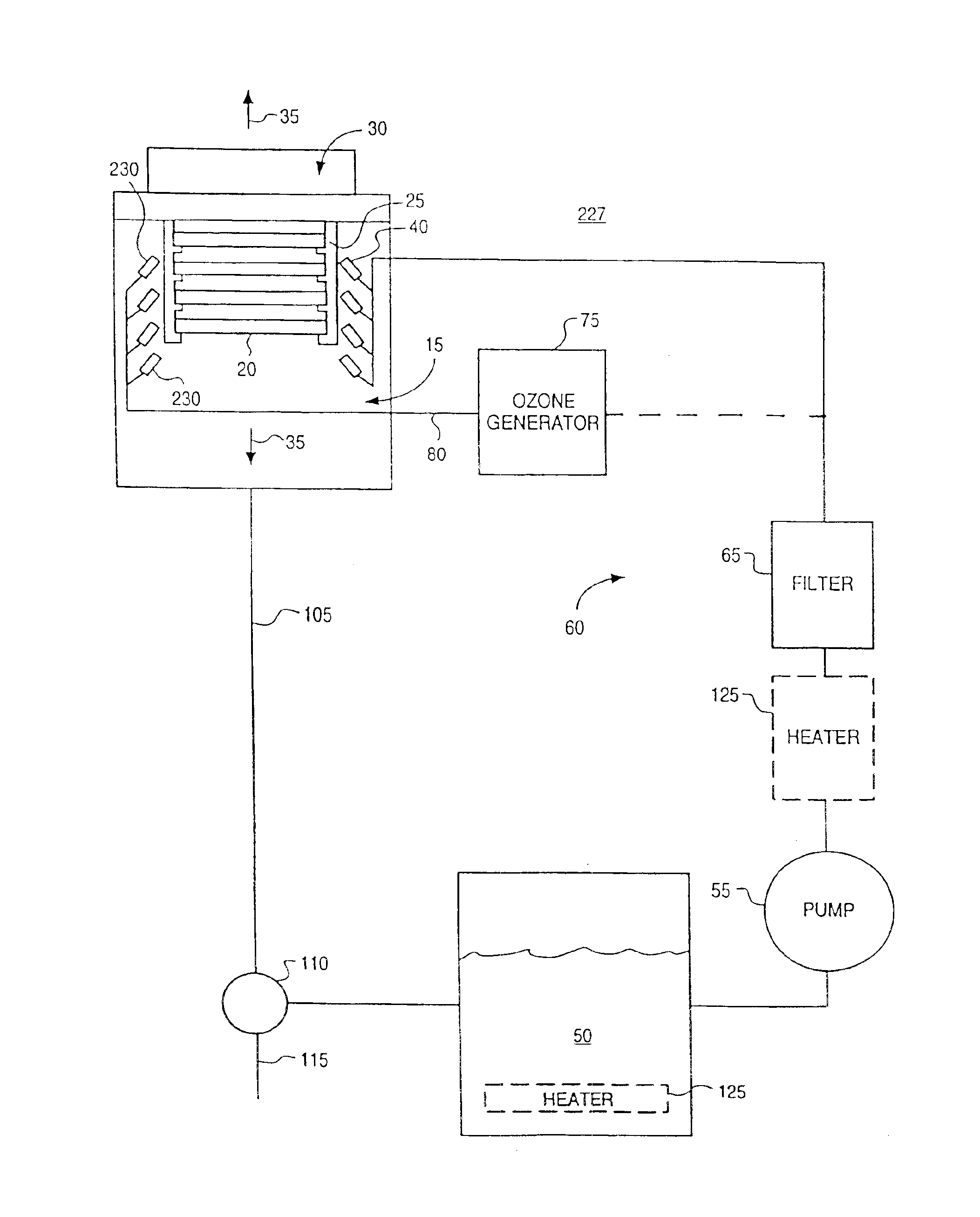
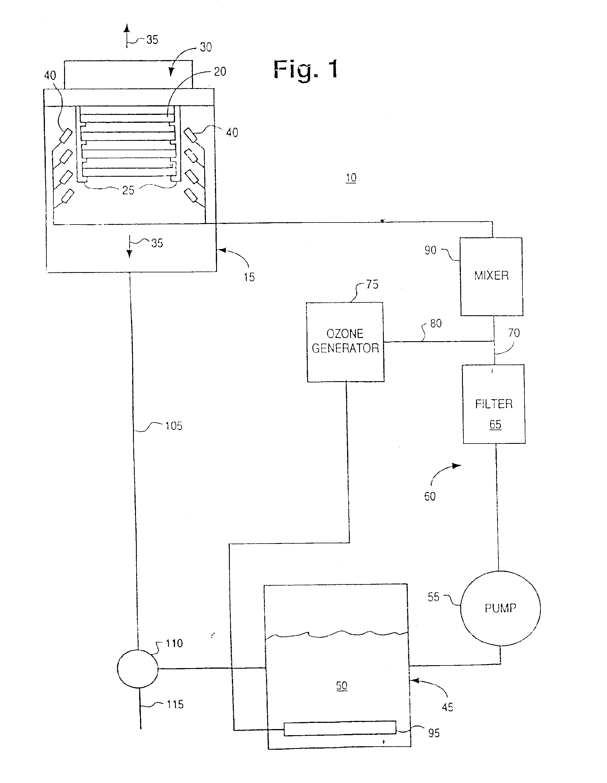
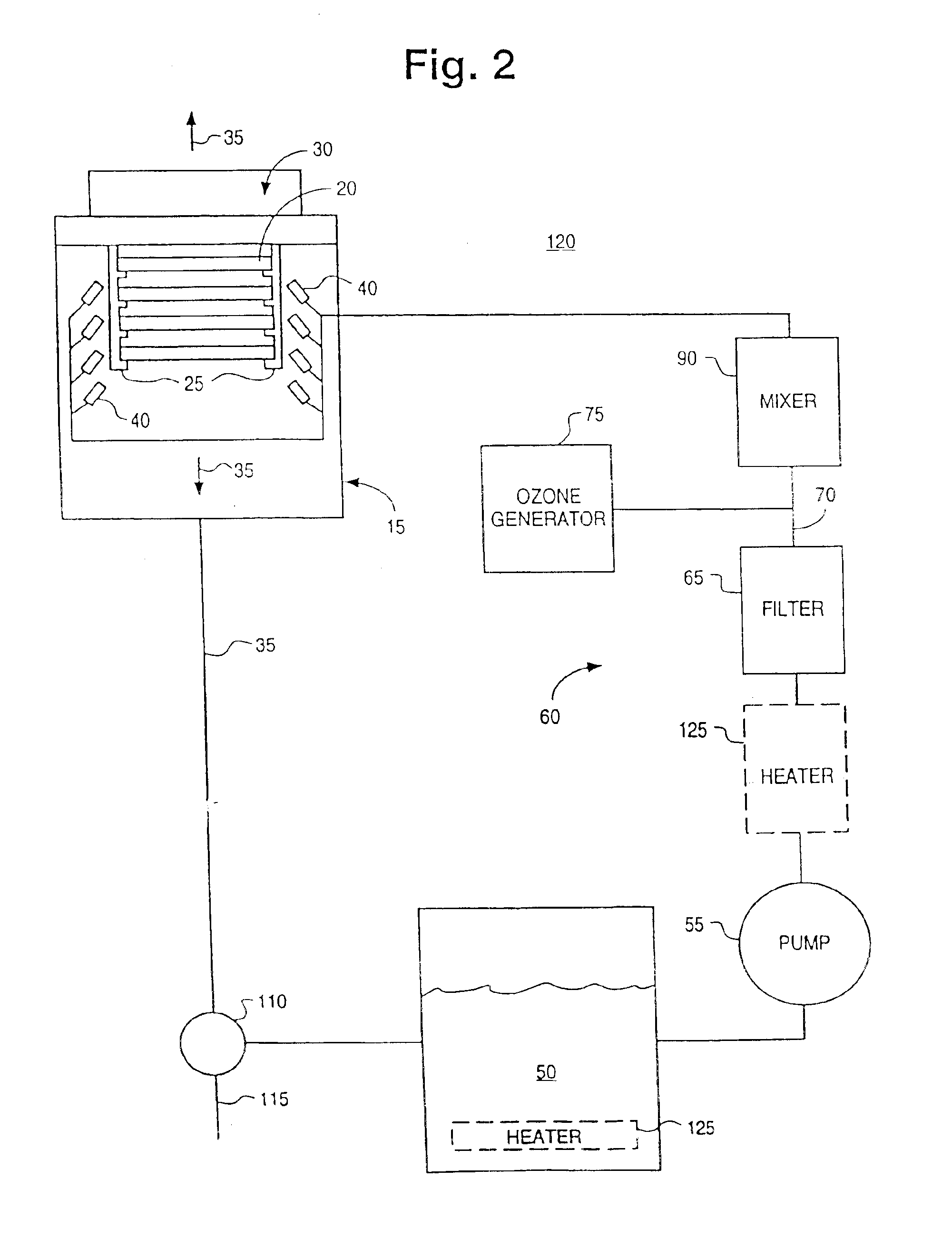
Apparatus for supplying a mixture of a treatment liquid and ozone for treatment of a surface of a workpiece, such as a semiconductor workpiece, to execute the foregoing processes are set forth below. The preferred embodiment of the apparatus comprises a liquid supply line that is used to provide fluid communication between a reservoir containing the treatment liquid and a treatment chamber housing the semiconductor workpiece. A heater heats the workpiece, either directly or indirectly. Preferably, the workpiece is heated by heating the treatment liquid that is supplied to the workpiece. One or more nozzles accept the treatment liquid from the liquid supply line and spray it onto the surface of the workpiece while an ozone generator provides ozone into an environment containing the workpiece.

Referring to FIG. 1, the treatment system, shown generally at 10, includes a treatment chamber 15 that contains one or more workpieces 20, such as semiconductor wafer workpieces. Although the ill...


PUM

PropertyMeasurementUnit
temperatureaaaaaaaaaa

Abstract

A novel chemistry, system and application technique reduces contamination of semiconductor wafers and similar substrates and enhances and expedites processing. A stream of liquid chemical is applied to the workpiece surface. Ozone is delivered either into the liquid process stream or into the process environment. The ozone is preferably generated by a high capacity ozone generator. The chemical stream is provided in the form of a liquid or vapor. A boundary layer liquid or vapor forms on the workpiece surface. The thickness of the boundary layer is controlled. The chemical stream may include ammonium hydroxide for simultaneous particle and organic removal, another chemical to raise the pH of the solution, or other chemical additives designed to accomplish one or more specific cleaning steps.

Description

FIELD OF THE INVENTIONThe cleaning of semiconductor wafers is often a critical step in the fabrication processes used to manufacture integrated circuits or the like. The geometries on wafers are often on the order of fractions of a micron, while the film thicknesses may be on the order of 20 Angstroms. This renders the devices highly susceptible to performance degradation due to organic, particulates or metallic / ionic contamination. Even silicon dioxide, which is used in the fabrication structure, can be considered a contaminant if the quality or thickness of the oxide does not meet design parameters.Although wafer cleaning has a long history, the era of “modern” cleaning techniques is generally considered to have begun in the early 1970s when RCA developed a cleaning sequence to address the various types of contamination. Although others developed the same or similar processes in the same time frame, the general cleaning sequence in its final form is basically the same.The first st...

Claims


Application Information

Patent Timeline
Patent Type & Authority Patents(United States)
IPC IPC(8): B08B3/08B08B3/02B08B3/04B08B3/00B08B7/00H01L21/00H01L21/02H01L21/306H01L21/3065H01L23/495H05K3/34
CPCB08B3/00B08B3/02B08B3/044B08B3/08B08B7/00H01L21/02052H01L21/02054H01L21/3065H01L21/6704H01L21/67051H01L23/49582H05K3/3426H01L2924/0002B08B2203/005B08B2203/007B08B2230/01Y10S134/902H01L2924/00Y02P70/50
Inventor BERGMAN, ERIC J.
Owner OEM GRP LLC
Why Eureka
Try Eureka