Method for processing a wafer and apparatus for performing the same

a technology of wafers and processing methods, applied in the direction of coatings, chemical vapor deposition coatings, plasma techniques, etc., can solve the problems of lowering the operation speed and reliability of a semiconductor device, affecting the etching of the native oxide layer other structures integrated on the wafer may also be affected by the wet etching method, so as to achieve easy etching and maximize production efficiency

Inactive Publication Date: 2005-03-22
SAMSUNG ELECTRONICS CO LTD
View PDF18 Cites 34 Cited by
  • Summary
  • Abstract
  • Description
  • Claims
  • Application Information

AI Technical Summary

Benefits of technology

According to the present invention, a wafer is processed by adjusting the temperature appropriately within the same space. Particularly, since a plurality of wafers may be processed simultaneously, a producing efficiency is improved.
According to the present invention, a predetermined material formed on a plurality of wafers may be easily etched within the same space to maximize production efficiency.

Problems solved by technology

It also becomes a cause of increasing contact resistance, which leads to a lowering of an operation speed and the reliability of a semiconductor device.
However, for a contact hole having a high aspect ratio, the etching of the native oxide layer by the wet etching method is not easy.
In addition, other structures integrated on the wafer may also be affected by the wet etching method due to some of the chemicals used in the wet etching method.
Since the wafer is processed through a single wafer-type treatment method according to the dry etching method, however, the processing efficiency of the etching of the native oxide layer is very low.
The growth of the native oxide layer, however, cannot be completely restrained through implementing the pre-treating process steps.
However, the chamber has a spatial limitation and so the manufacturing cost of the chamber increases.

Method used


Image

  • Method for processing a wafer and apparatus for performing the same
  • Method for processing a wafer and apparatus for performing the same
  • Method for processing a wafer and apparatus for performing the same

Examples


Embodiment Construction

Korean Patent Application No. 2001-59323, filed Sep. 25, 2001, and entitled: “Method for Processing Wafer and Apparatus for Performing the Same,” is incorporated by reference herein in its entirety.

Hereinafter, the embodiments of the present invention will be described in detail with reference to the accompanying drawings.

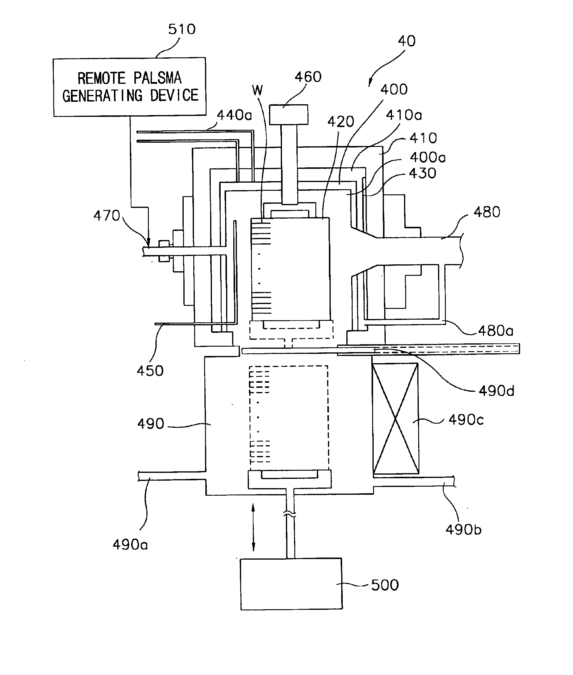
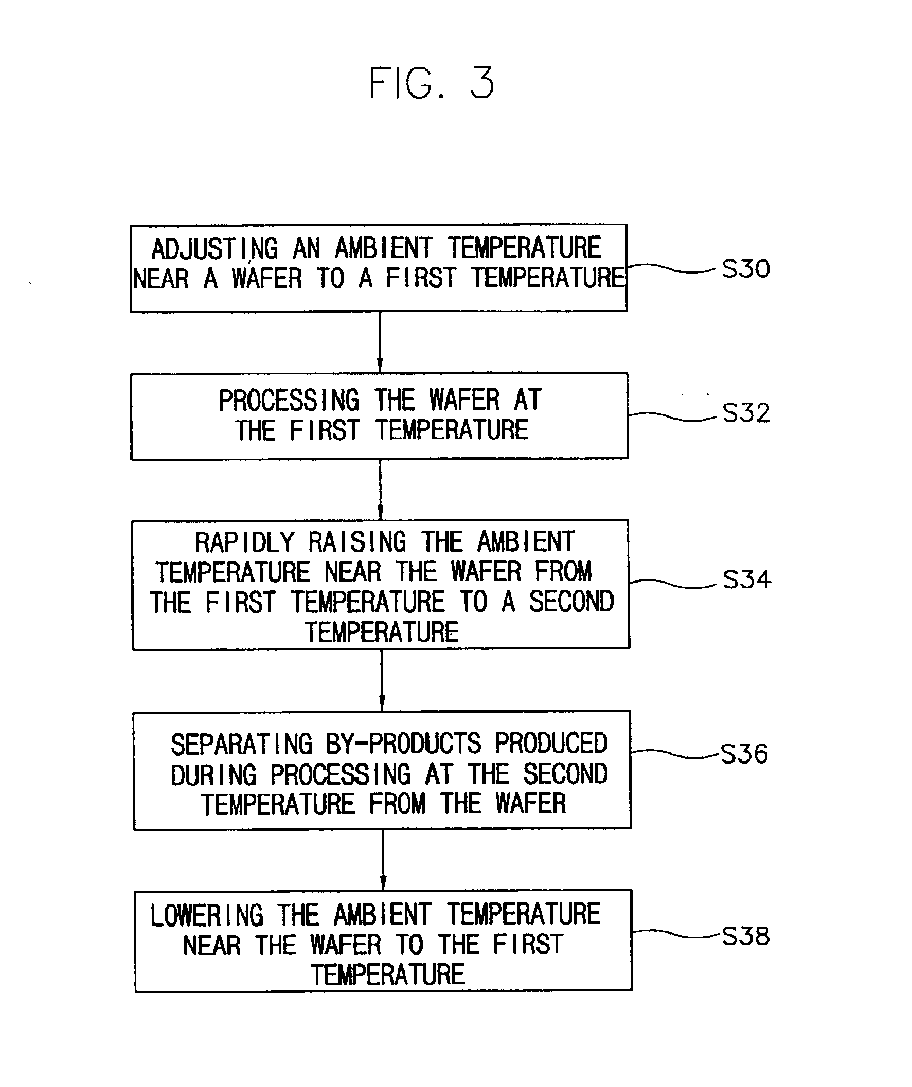
FIG. 3 is a flow chart of a wafer processing method according to an embodiment of the present invention.

Referring to FIG. 3, in step S30, an ambient temperature near a wafer is adjusted to a first temperature. Preferably, the first temperature for removing a native oxide layer is adjusted to about 15-30° C. The temperature is adjusted using a cooling agent. As for the cooling agent, liquefied nitrogen, carbon dioxide, water, or the like may be used. Either one cooling agent or a mixture form of more than one cooling agents can be used.

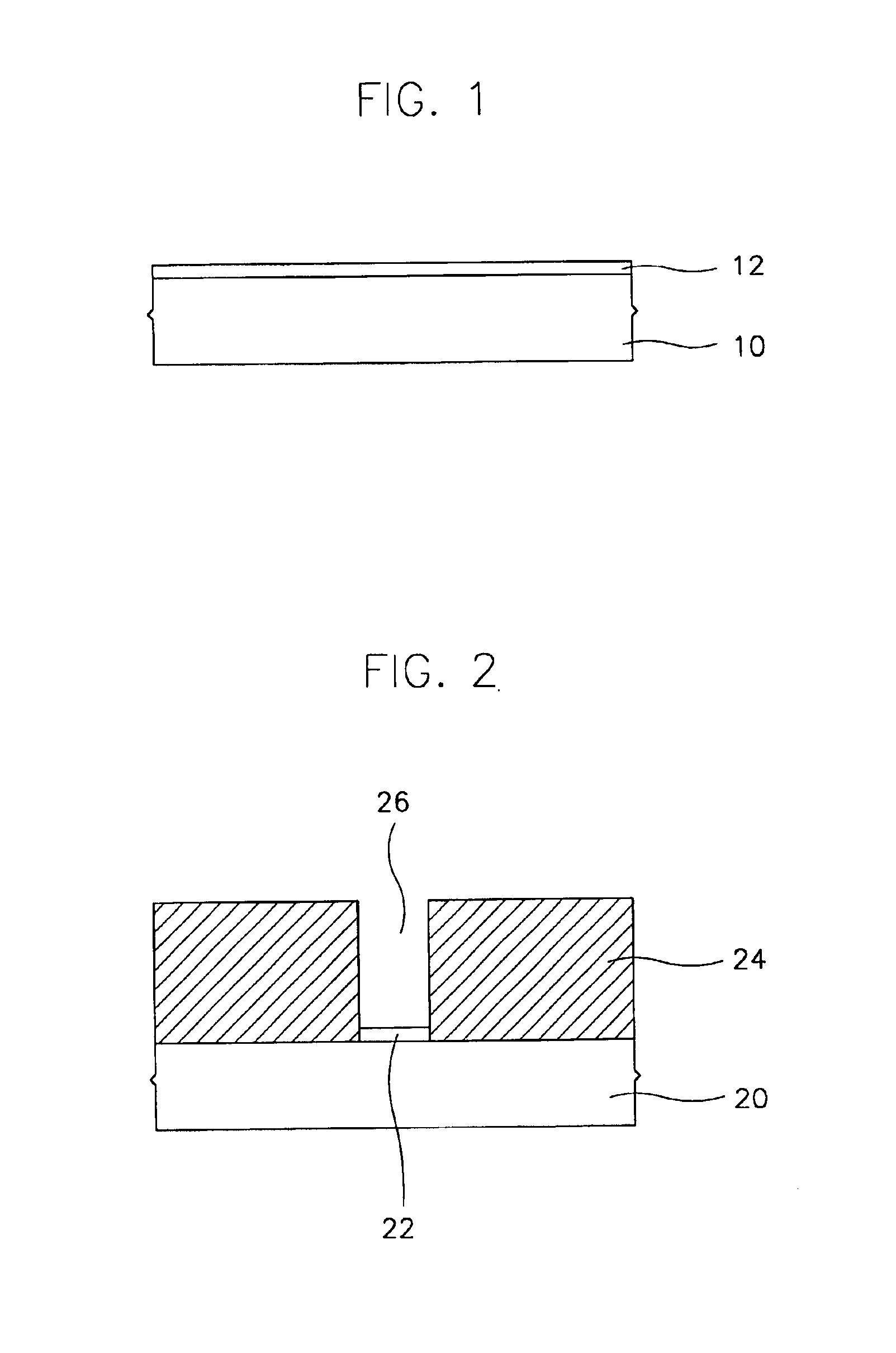
In the next step, S32, the wafer is processed at the first temperature. For example, a material such as a native oxide layer formed ...


PUM

PropertyMeasurementUnit
temperatureaaaaaaaaaa

Abstract

Disclosed are a method and an apparatus for processing a wafer in manufacturing a semiconductor device and a method and an apparatus for etching a material formed on the wafer, wherein first and second cooling parts adjust an ambient temperature near a plurality of wafers to a first temperature, the wafers are processed by introducing a reaction gas at the first temperature, then, a heating part rapidly raises the temperature of the atmosphere near the wafers from the first temperature to the second temperature to partially separate by-products produced during the processing, the second temperature is maintained to separate most of the by-products from the wafers, and the processing steps are implemented in-situ within the same space. Accordingly, a native oxide layer formed on several wafers can be etched and the reaction by-products can be removed in-situ in the same chamber so productivity is improved.

Description

BACKGROUND OF THE INVENTION1. Field of the InventionThe present invention relates to a method for processing a wafer and an apparatus for performing the same. The present invention further relates to a method for etching a wafer and an apparatus for performing the same. More particularly, the present invention relates to a method for processing a material, such as a native oxide layer, formed on a wafer and a method for etching the material.2. Description of the Related ArtRecently, the design of semiconductor devices has made rapid progress for wide spread use in information media applications such as computers. In particular, this progress has required the semiconductor devices to function at a high operating speed and to have a large storage capacitance. In order to satisfy these requirements, semiconductor devices having an increased density, higher reliability, and a faster response time are under continued development.The continuous development of manufacturing techniques of a...

Claims


Application Information

Patent Timeline
Patent Type & Authority Patents(United States)
IPC IPC(8): H01L21/00H01L21/02H01L21/306H01L21/311H01L21/3065H01L21/304
CPCH01L21/02046H01L21/67109H01L21/31116H01L21/3065
Inventor LEE, KWANG-MYUNGTAKAGI, MIKIOAN, JAE-HYUKCHAE, SEUNG-KIKIM, JEA-WOOK
Owner SAMSUNG ELECTRONICS CO LTD
Why Eureka
Try Eureka