Adhesion by plasma conditioning of semiconductor chip surfaces

a technology of semiconductor chip and surface, which is applied in the direction of semiconductor devices, semiconductor/solid-state device details, electrical apparatus, etc., can solve the problems of unresolved technology of reliable adhesion of the underfill material to the semiconductor chip and to the various substrates employed, and create a gap between the chip and the substrate, etc., to improve the surface affinity to adhesion, improve the adhesion, and clean the polymer surface

Inactive Publication Date: 2005-03-22
TEXAS INSTR INC
View PDF23 Cites 37 Cited by
  • Summary
  • Abstract
  • Description
  • Claims
  • Application Information

AI Technical Summary

Benefits of technology

The present invention describes a plasma conditioning method of improving the adhesion between an integrated circuit chip, having active and passive surfaces, the active surface polymer-coated and having a plurality of electrical coupling members, and an insulating underfill material. The method comprises the steps of positioning a wafer having a plurality of integrated circuits, including the coupling members, in a vacuum chamber of a plasma apparatus so that the polymer-coated surface faces the plasma source. Next, a plasma is initiated; the ion mean free path is controlled so that the ions reach the wafer surface with predetermined energy. The wafer surface is then exposed to the plasma for a length of time sufficient to roughen the polymer surface, clean the polymer surface from organic contamination and improve the surface affinity to adhesion. The adhesion ability of this surface to organic underfill material is thus enhanced.
The effect of the plasma conditioning results in a mechanical roughening of the polymer coat surface, as clearly visible in microscopic examination; further in a cleaning of that surface, especially from organic contamination, as clearly measured by the contact angle of a water drop on the surface. In addition, the polymer coat surface chemistry is modified and the surface energy increased. Together, these combined effects provide an improved adhesion capability of the polymer coat surface for underfill material, which is employed after flip-chip assembly of the semiconductor chip.

Problems solved by technology

These solder balls thus create a gap between chip and substrate.
It was found that the mismatch of thermal expansion coefficients between the semiconductor chip (usually silicon) and the substrate (usually ceramic or laminated plastic) causes strain and resultant stress in the coupling members (usually solder balls) and their joints.
The problem of reliable adhesion of the underfill material to the semiconductor chip and to the various substrates employed has not been addressed in known technology.

Method used


Image

  • Adhesion by plasma conditioning of semiconductor chip surfaces
  • Adhesion by plasma conditioning of semiconductor chip surfaces
  • Adhesion by plasma conditioning of semiconductor chip surfaces

Examples


first embodiment

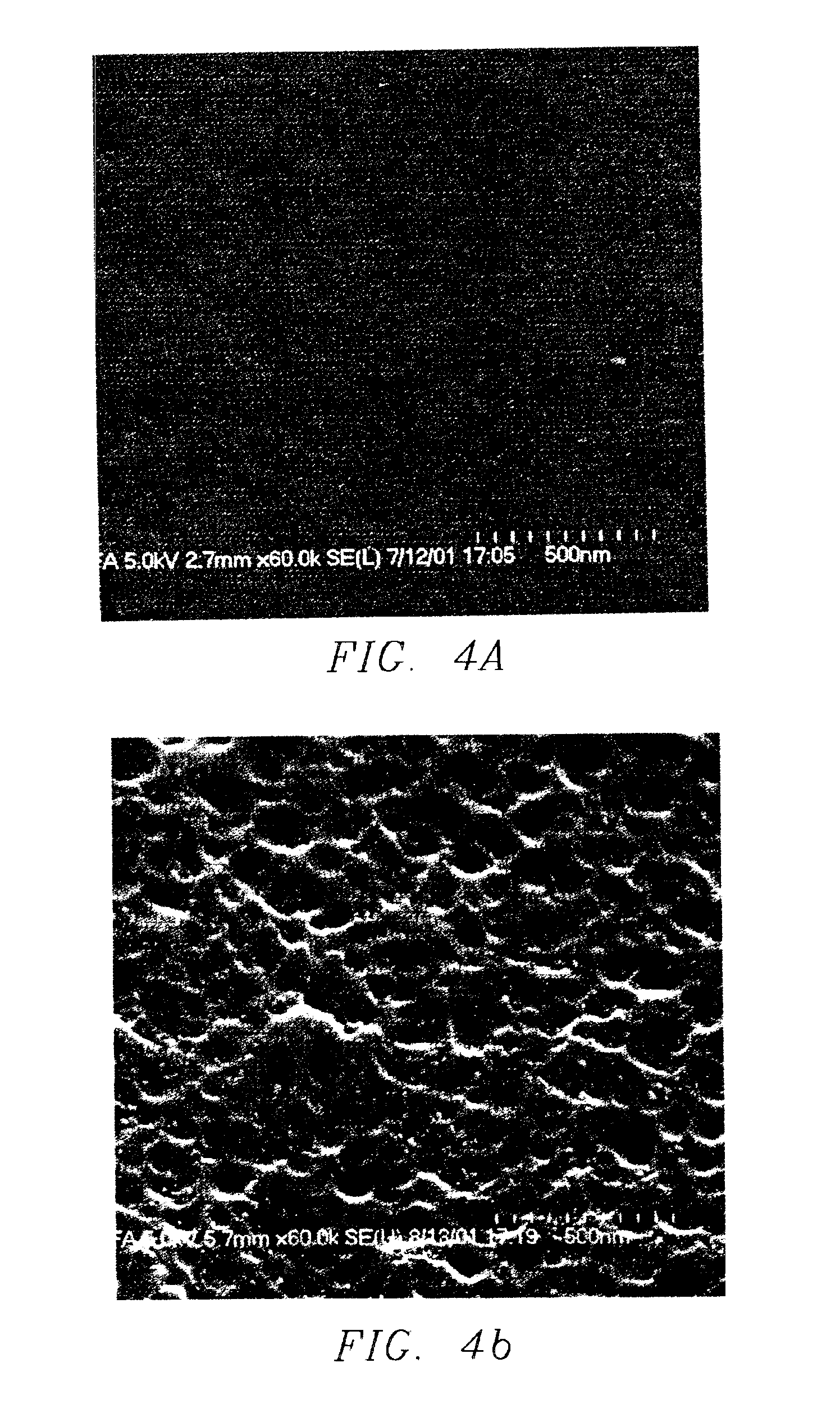
FIGS. 7A and 7B describe the structure of negative photosensitive polyimide in the polymer coat over the active chip surface. FIG. 7A, applicable to the ester type of polyimide, shows the photoreactive group indicated by “P”. Enhancing the number of “dangling bonds” and adhesion sites by the plasma conditioning contributes to the improved surface affinity to adhesion.

FIG. 7B, applicable to the ionic type of polyimide, shows the electrical charges involved in the locations of ionic binding. Here again, “P” indicates the photoreactive group. Enhancing the number of “dangling bonds” and adhesion sites by the plasma conditioning contributes to the improved surface affinity to adhesion.

second embodiment

FIG. 8 describes the formation of poly-benzoxasol in the polymer coat over the active chip surface. The formula shows the base polymer as the precursor of the CRC-8000 series. Heat treatment is then transforming the base polymer into poly-benzoxasole as the post-bake formulation of the polymer.

FIGS. 9 to 11 are schematic cross sections of a number of different plasma apparatus, and thus plasma processes, which are all suitable for the plasma conditioning of whole semiconductor wafers according to the present invention. It should be stressed that the plasma conditioning method of the present invention is equally successful for whole wafers before “sawing” into individual chips, or after singulation into individual chips. In the latter case, the plurality of chips remains still attached to the supporting tape (the so-called “blue tape” held within a sturdy frame).

The apparatus of FIG. 9 is referred to as a “reactive ion etch asher”. In FIG. 9, inside the bell jar 901 are the pedestal ...


PUM


Abstract

A plasma conditioning method of improving the adhesion between an integrated circuit chip, having active and passive surfaces, the active surface polymer-coated and having a plurality of electrical coupling members, and an insulating underfill material. The method comprises the steps of positioning a wafer having a plurality of integrated circuits, including the coupling members, in a vacuum chamber of a plasma apparatus so that the polymer-coated surface faces the plasma source. Next, a plasma is initiated; the ion mean free path is controlled so that the ions reach the wafer surface with predetermined energy. The wafer surface is then exposed to the plasma for a length of time sufficient to roughen the polymer surface, clean the polymer surface from organic contamination and improve the surface affinity to adhesion. The adhesion ability of this surface to organic underfill material is thus enhanced.

Description

FIELD OF THE INVENTIONThe present invention is related in general to the field of electronic systems and semiconductor devices and more specifically to the field of flip-chip assembly with underfilling, in which strong adhesion is required between the underfilling material, the semiconductor chip and the substrate.DESCRIPTION OF THE RELATED ARTIn flip-chip assembly, the active surface of a semiconductor chip, including the integrated circuits, is connected face-down to the substrate by coupling members, usually solder balls attached, on one side, to the chip and, on the opposite side, to the substrate. These solder balls thus create a gap between chip and substrate.Important aspects of the flip-chip assembly of semiconductor chips have been studied in the 1960's by IBM researchers and published in a series of papers (IBM Journal for Research and Development, vol. 13, pp. 226-296, May 1969). It was found that the mismatch of thermal expansion coefficients between the semiconductor ch...

Claims


Application Information

Patent Timeline
Patent Type & Authority Patents(United States)
IPC IPC(8): H01L21/56H01L21/60H01L21/02H01L23/31H01L23/28H01L23/485H01L23/48H01L21/44H01L21/48H01L21/50
CPCH01L21/563H01L23/3142H01L24/03H01L24/05H01L24/11H01L23/3128H01L24/13H01L2924/0002H01L23/4334H01L2224/0401H01L2224/05624H01L2224/13099H01L2224/131H01L2224/45144H01L2224/73203H01L2224/73204H01L2924/01004H01L2924/01005H01L2924/01006H01L2924/01007H01L2924/01013H01L2924/01014H01L2924/01015H01L2924/01018H01L2924/01028H01L2924/01029H01L2924/01032H01L2924/01046H01L2924/01047H01L2924/01049H01L2924/0105H01L2924/01074H01L2924/01079H01L2924/01082H01L2924/01322H01L2924/01327H01L2924/014H01L2924/05042H01L2924/12044H01L2924/14H01L2924/15311H01L2224/04042H01L2924/10253H01L2224/48624H01L2224/05027H01L24/45H01L2224/05022H01L2224/13023H01L2224/13109H01L2224/16225H01L2224/32225H01L2924/01023H01L2924/01033H01L2924/01087H01L2224/13006H01L2224/05572H01L2224/45124H01L2924/00014H01L2924/00012H01L2924/00H01L2224/05552H01L2924/181H01L2224/48724H01L2224/05559H01L21/44H01L21/48H01L21/60
Inventor COWENS, MARVIN W.MURTUZA, MASOODYAMUNAN, VINUODEGARD, CHARLESCOFFMAN, PHILLIP R.
Owner TEXAS INSTR INC
Why Eureka
Try Eureka