Maskless reflection electron beam projection lithography

a technology of electron beam and beam projection, applied in the field of semiconductor manufacturing, can solve the problems of insufficient economic preparation of customer-specific circuits in small numbers, and the process is very time-consuming

Active Publication Date: 2005-03-22
KLA TENCOR TECH CORP
View PDF16 Cites 91 Cited by
  • Summary
  • Abstract
  • Description
  • Claims
  • Application Information

AI Technical Summary

Problems solved by technology

However, it is disadvantageous that the process is very time-consuming, due to the sequential, point-wise writing.
Disadvantages of conventional electron beam projection lithography systems includes that a corresponding mask is necessary for each structure to be exposed.
The preparation of customer-specific circuits in small numbers is not economic, because of the high costs associated with mask production.

Method used


Image

  • Maskless reflection electron beam projection lithography
  • Maskless reflection electron beam projection lithography
  • Maskless reflection electron beam projection lithography

Examples


Embodiment Construction

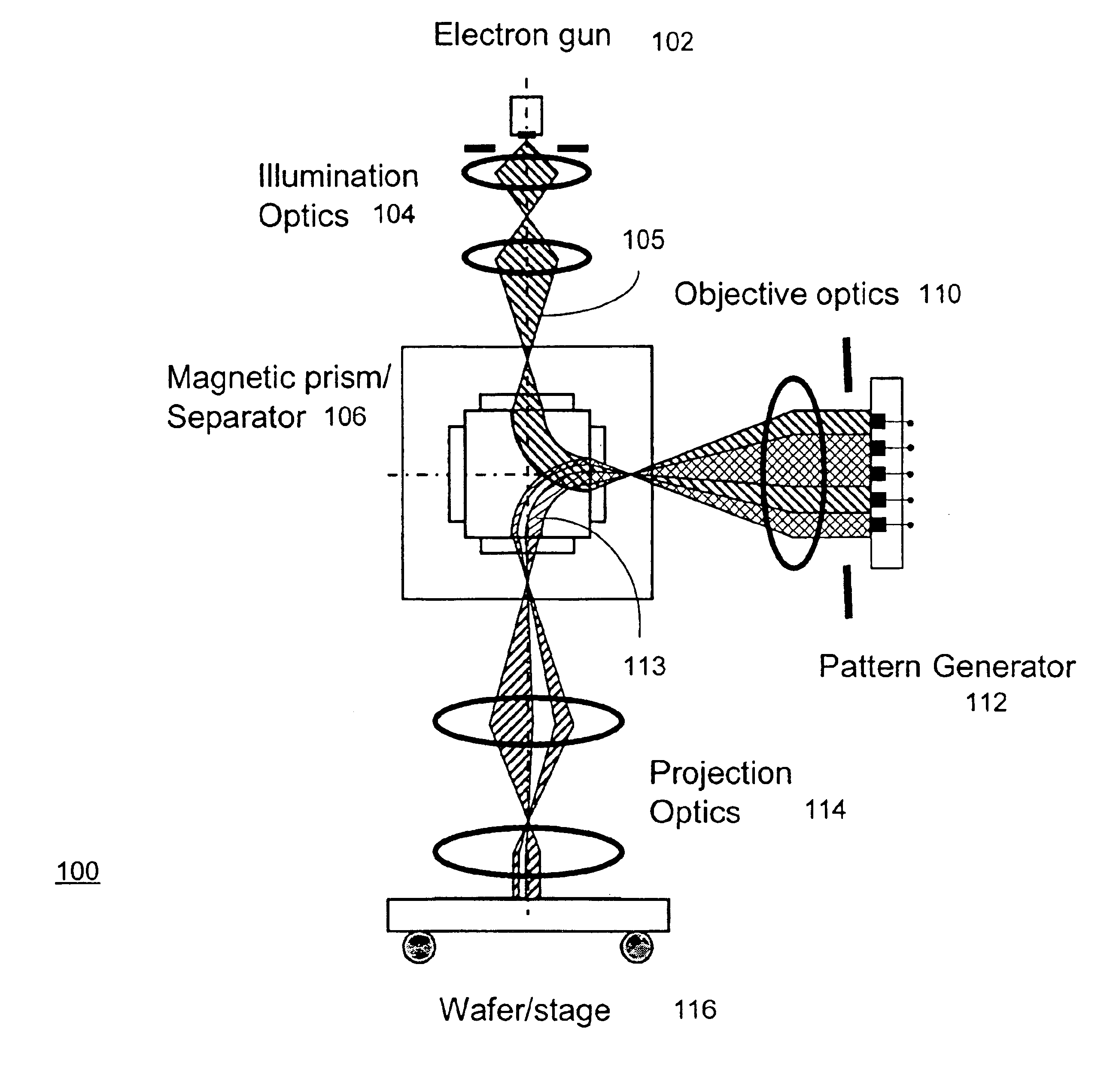
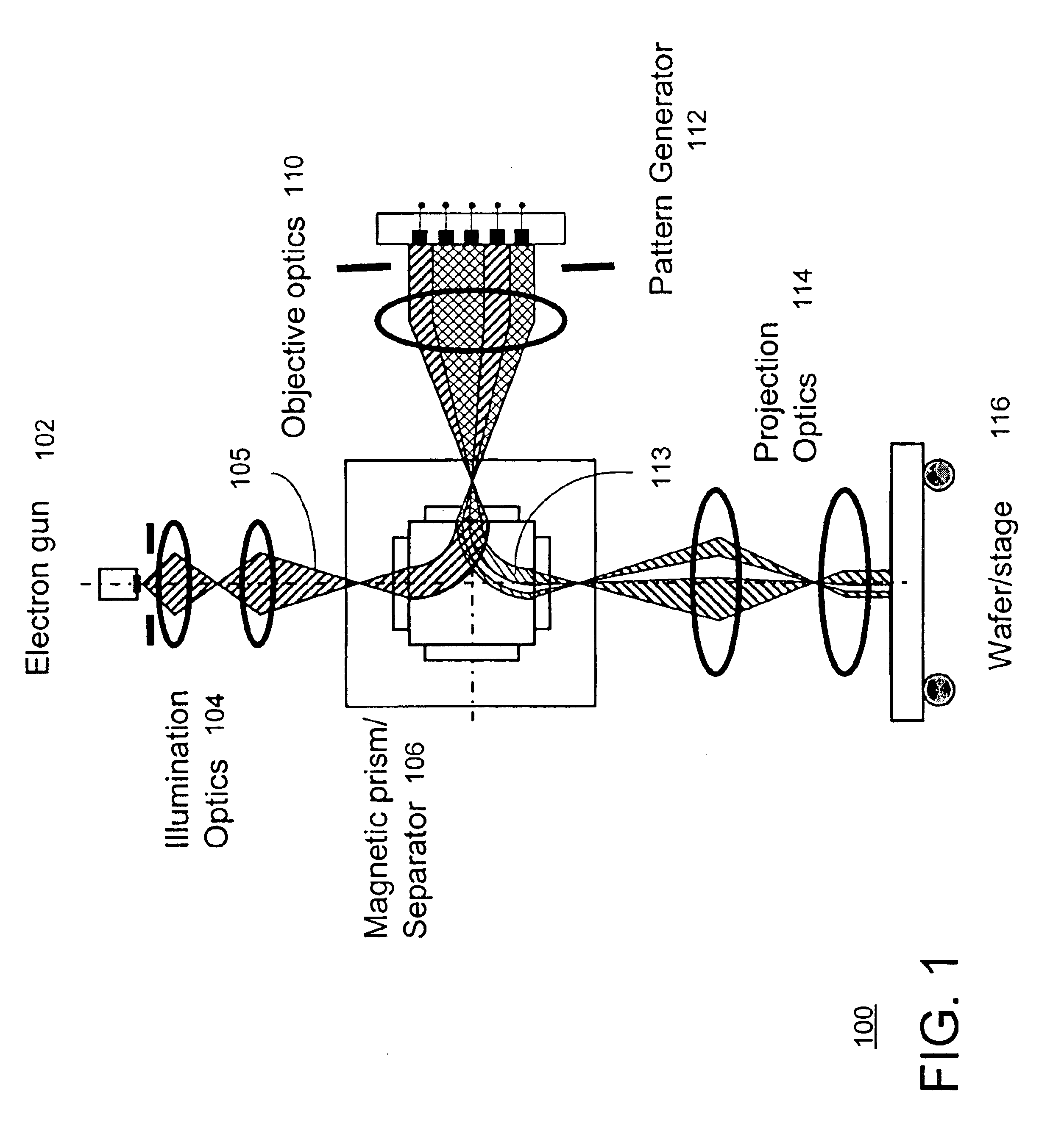
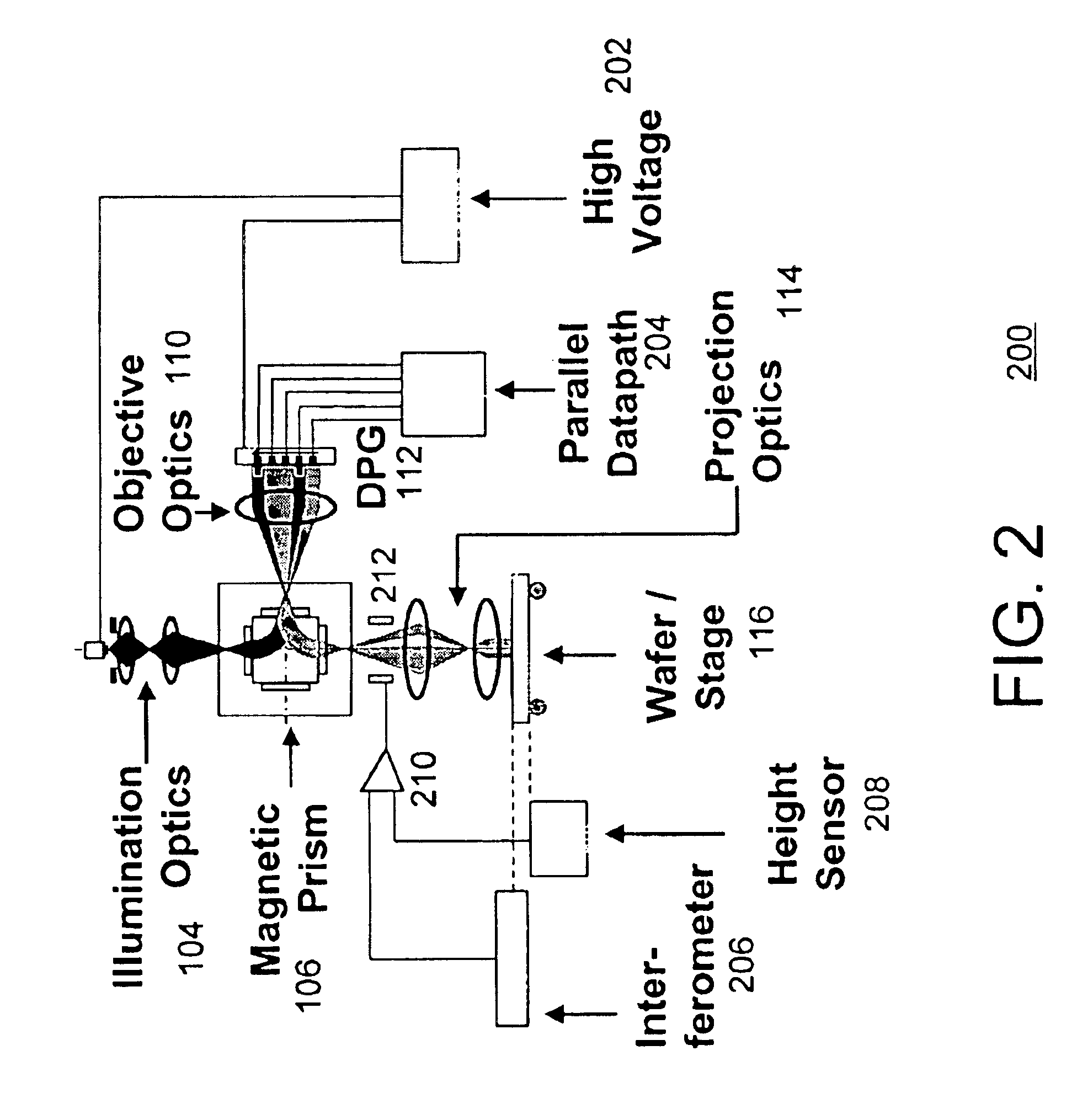
As discussed above, electron-beam direct write (EBDW) lithography has the potential to achieve excellent resolution. However, EBDW has a traditional problem relating to its low throughput. For example, it may take ten to one hundred hours to inscribe an entire wafer using EBDW lithography. One previous approach to attempt to increase the throughput is by increasing the beam current. However, when the current density exceeds a certain threshold, electron-electron interactions cause the beam to blur.

This patent application discloses a system and method of electron beam lithography that overcomes the above-discussed disadvantages and problems. Rather than focusing the electron beam into a tiny spot, the approach described herein floods the wafer with the electron beam. This enables use of a high beam current while keeping the beam current density at a level consistent with minimal electron-electron interactions. For example, an area roughly 0.1 millimeters (mm) wide may be illuminated....


PUM

PropertyMeasurementUnit
operating voltageaaaaaaaaaa
sizeaaaaaaaaaa
voltageaaaaaaaaaa

Abstract

One embodiment disclosed relates to an apparatus for reflection electron beam lithography. An electron source is configured to emit electrons. The electrons are reflected to a target substrate by portions of an electron-opaque patterned structure having a lower voltage level and are absorbed by portions of the structure having a higher voltage level. Another embodiment relates to a novel method of electron beam lithography. An incident electron beam is formed and directed to an opaque patterned structure. Electrons are reflected from portions of the structure having a lower voltage level applied thereto and are absorbed by portions of the structure having a higher voltage level applied thereto. The reflected electrons are directed towards a target substrate to form an image and expose a lithographic pattern.

Description

BACKGROUND OF THE INVENTION1. Field of the InventionThe present invention relates generally to semiconductor manufacturing and related technologies. More particularly, the present invention relates to electron beam lithography.2. Description of the Background ArtAs is well-understood in the art, a lithographic process includes the patterned exposure of a resist so that portions of the resist can be selectively removed to expose underlying areas for selective processing such as by etching, material deposition, implantation and the like. Traditional lithographic processes utilize electromagnetic energy in the form of ultraviolet light for selective exposure of the resist. As an alternative to electromagnetic energy (including x-rays), charged particle beams have been used for high resolution lithographic resist exposure. In particular, electron beams have been used since the low mass of electrons allows relatively accurate control of an electron beam at relatively low power and relati...

Claims


Application Information

Patent Timeline
Patent Type & Authority Patents(United States)
IPC IPC(8): H01J37/317G03F1/00G03F7/20
CPCB82Y10/00H01J37/3174B82Y40/00H01J2237/31789
Inventor MANKOS, MARIANHESS, HARALD F.ADLER, DAVID L.BERTSCHE, KIRK J.
Owner KLA TENCOR TECH CORP
Why Eureka
Try Eureka