Repeated structure of nanometer thin films with symmetric or asymmetric configuration for SPR signal modulation

a nanometer thin film and signal modulation technology, applied in the field of biomedical chips, can solve the problems of inconvenient use, difficult calibration and measurement with scanning mechanism, etc., and achieve the effect of reducing drawbacks and improving the efficiency of angular interrogation

Inactive Publication Date: 2005-03-22
NAT TAIWAN UNIV
View PDF0 Cites 7 Cited by
  • Summary
  • Abstract
  • Description
  • Claims
  • Application Information

AI Technical Summary

Benefits of technology

The present invention offers a novel construction of dielectric coupler, which substantially reduces the drawbacks of the existing devices, while tremendously improves the efficiency of the angular interrogation of mechanism and wavelength interrogation applications. With regard to the sensing of common SPR chips, the resonant angle after coated with a metal layer is usually about 74 deg in air, while 87 deg in liquid, which is difficult in calibration and measurement with scanning mechanism and inconvenient to use. The multilayer structure of this present invention enables a square-wave grating coupler based SPR system, through the adjustment of refractive index and thickness of the material, the resonance of wavelength and angular can be achieved.

Problems solved by technology

With regard to the sensing of common SPR chips, the resonant angle after coated with a metal layer is usually about 74 deg in air, while 87 deg in liquid, which is difficult in calibration and measurement with scanning mechanism and inconvenient to use.

Method used


Image

  • Repeated structure of nanometer thin films with symmetric or asymmetric configuration for SPR signal modulation
  • Repeated structure of nanometer thin films with symmetric or asymmetric configuration for SPR signal modulation
  • Repeated structure of nanometer thin films with symmetric or asymmetric configuration for SPR signal modulation

Examples


Embodiment Construction

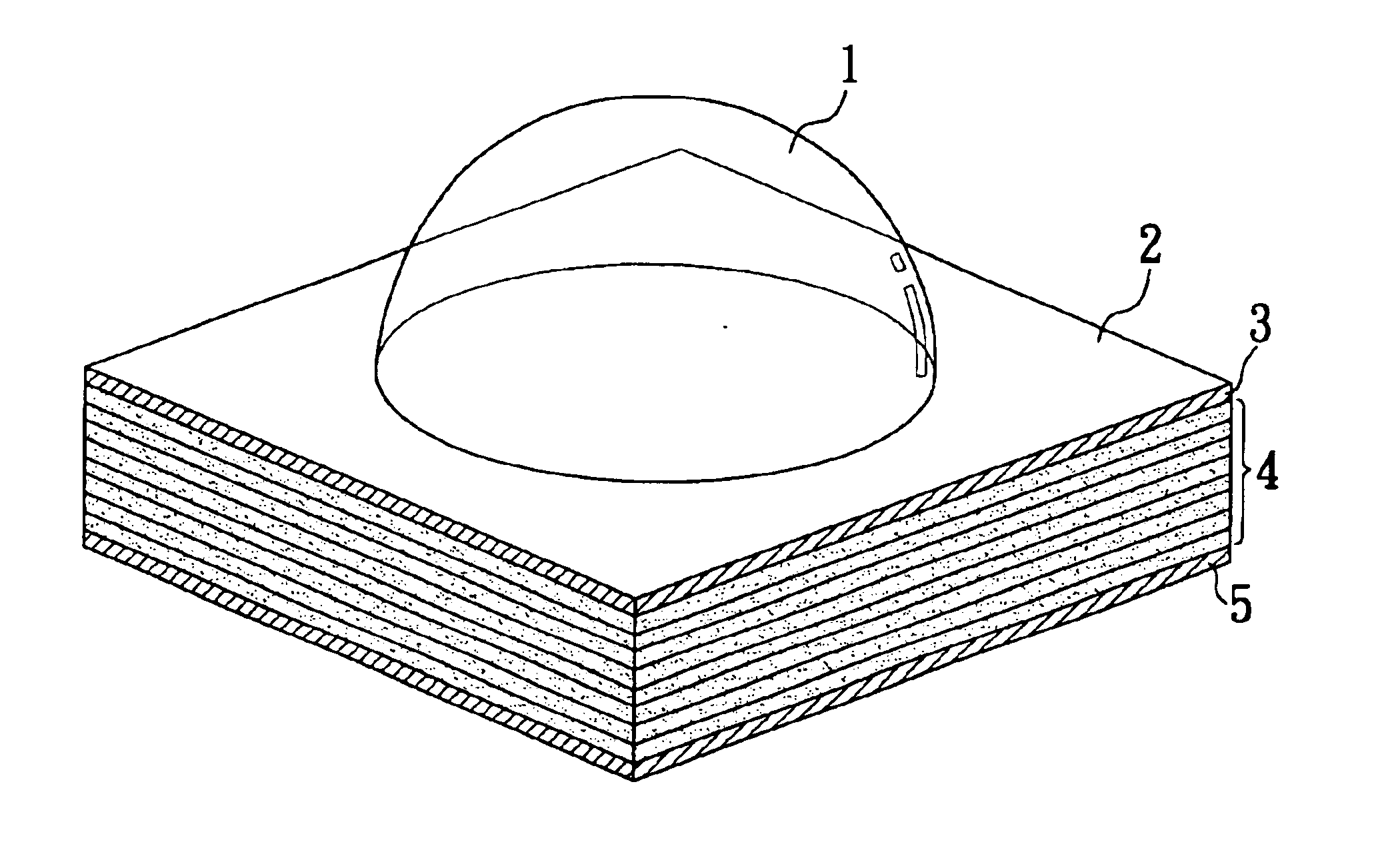
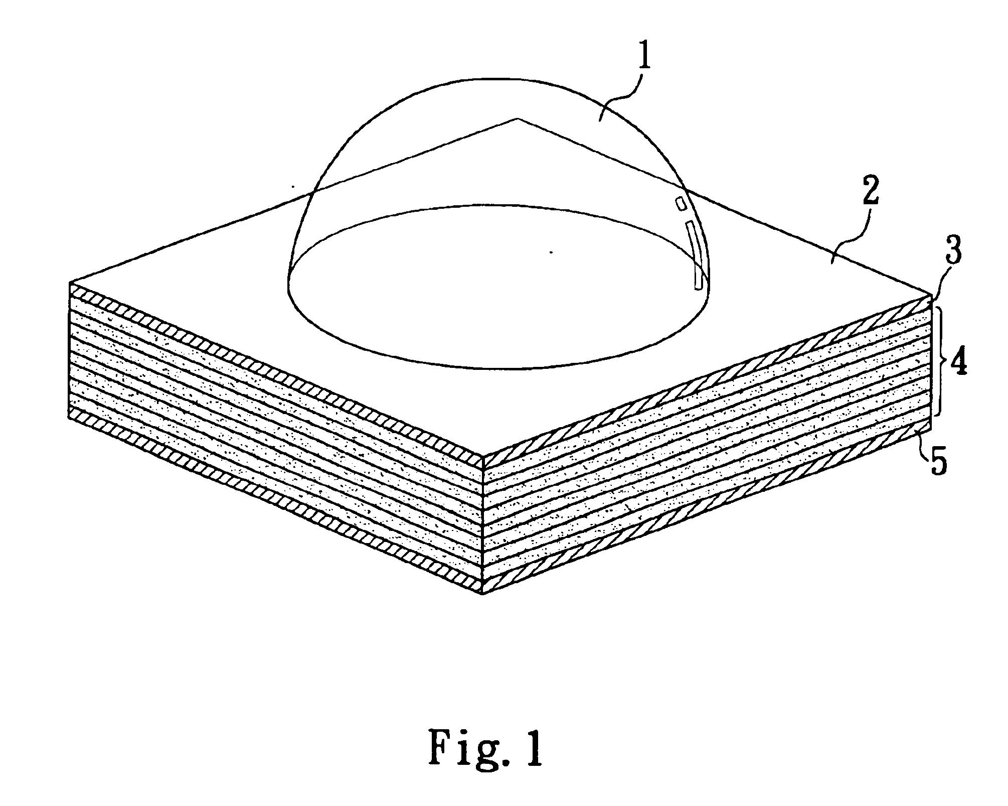
Embodiments of the present invention will now be described through a symmetric or asymmetric multilayer structure in an active surface plasmon resonance (SPR) chip, with reference to the accompanying figures. Referring first to FIG. 1, a symmetric or asymmetric multilayer structure in an active surface plasmon resonance (SPR) chip comprising: a prism 1, a substrate material 2, a thin gold film (can be other metal film) 3, a nanometer multilayer dielectric thin films 4, and a thin gold film 5.

The interposed stack of nanometer multilayer thin films is organized by the materials of a high and low refractive index alternately, and the thickness of each layer is set a fraction of wavelength of the incident light, which is about a tens to several hundreds of nanometers. Number of total layers is dependent on the equivalent refractive index as that in a single dielectric layer.

Material of a high or low refractive index can be viewed as a constituent of a “pair”, and a few pairs to tens of ...


PUM

PropertyMeasurementUnit
thicknessaaaaaaaaaa
refractive indexaaaaaaaaaa
thicknessaaaaaaaaaa

Abstract

A symmetric or asymmetric multilayer structure based on the technique of surface plasmon resonance (SPR) has been applied for modulation of resonant angle and wavelength. The fabrication of this invention can have nanoscale thin film layers up to several hundreds, while each layer has its own material of a high or low refractive index value, and the total layers in a thickness of tens to hundreds nanometers are grown in this single structure. This invention is intended for optimizing the scanning of mechanism by modulating SPR resonant angle and wavelength, and for developing the prospect of portable instruments.

Description

FIELD OF THE INVENTIONThe present invention relates generally to the research of a biomedical chip in sensing protein biomolecules by an optical method and more particularly relates to a procedure of coating a metal film on a surface plasmon resonance (SPR) device and a novel design of a multilayer structure.BACKGROUND OF THE INVENTIONDisregard the fact that quite a few patents on genetic engineering related techniques have raised many legal and ethical issues, human beings have indeed made a big progress in knowing their own origin during the last century. A widely recognized discovery is the rough draft of the human genome, or the molecular sequence of DNA that comprises the human genes. A biochip, known as DNA microarrays, was designed in the late of last century for accelerating genetic research. This new technology is expected to detect the presence of a whole array of genetically based diseases, and, moreover, to conduct widespread disease screening.A combination of molecular ...

Claims


Application Information

Patent Timeline
Patent Type & Authority Patents(United States)
IPC IPC(8): H01L31/00H01L33/00G01N21/55G01N21/75G01N21/77G02B6/122
CPCB82Y20/00G01N21/553G02B6/1226G01N21/554G01N2021/757Y10S977/719Y10S977/759Y10S977/792G01N2021/7776
Inventor LIN, CHII-WANNHUANG, CHEN KUNGLIN, SHIMINGLEE, CHIH KUNGCHANG, PEIZENLEE, SHU SHENG
Owner NAT TAIWAN UNIV
Why Eureka
Try Eureka