Oxide buffer layer for improved magnetic tunnel junctions

a buffer layer and tunnel junction technology, applied in the field of magnet film layers, can solve the problems of undesirable coupling, achieve the effects of reducing the grain size of the non-magnetic layer, and reducing the surface roughness

Inactive Publication Date: 2005-03-22
MICRON TECH INC
View PDF3 Cites 7 Cited by
  • Summary
  • Abstract
  • Description
  • Claims
  • Application Information

AI Technical Summary

Benefits of technology

The present invention seeks to mitigate problems caused by surface roughness in magnetoresistive device structures. A buffer layer is deposited and a non-magnetic barrier or spacer layer is grown on the buffer layer. Growing the non-magnetic layer on the buffer layer leads to decreased grain size of the non-magnetic layer. The decreased grain size provides a smoother surface. As a result, the surface will exhibit fewer extraneous magnetic dipoles and reduced inter-plane coupling. In general, the smoother surfaces will reduce topological magnetostatic interlayer coupling effects, such as Néel coupling.

Problems solved by technology

Such coupling typically is undesirable in magnetic elements because it creates the magnetic field bias offset in the response of the free layer to an external magnetic field.

Method used


Image

  • Oxide buffer layer for improved magnetic tunnel junctions
  • Oxide buffer layer for improved magnetic tunnel junctions
  • Oxide buffer layer for improved magnetic tunnel junctions

Examples


Embodiment Construction

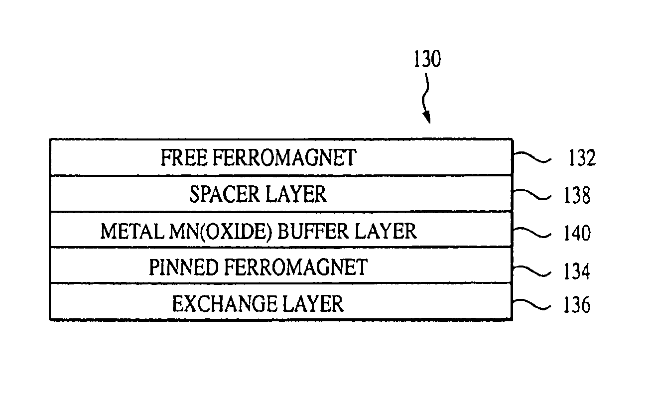
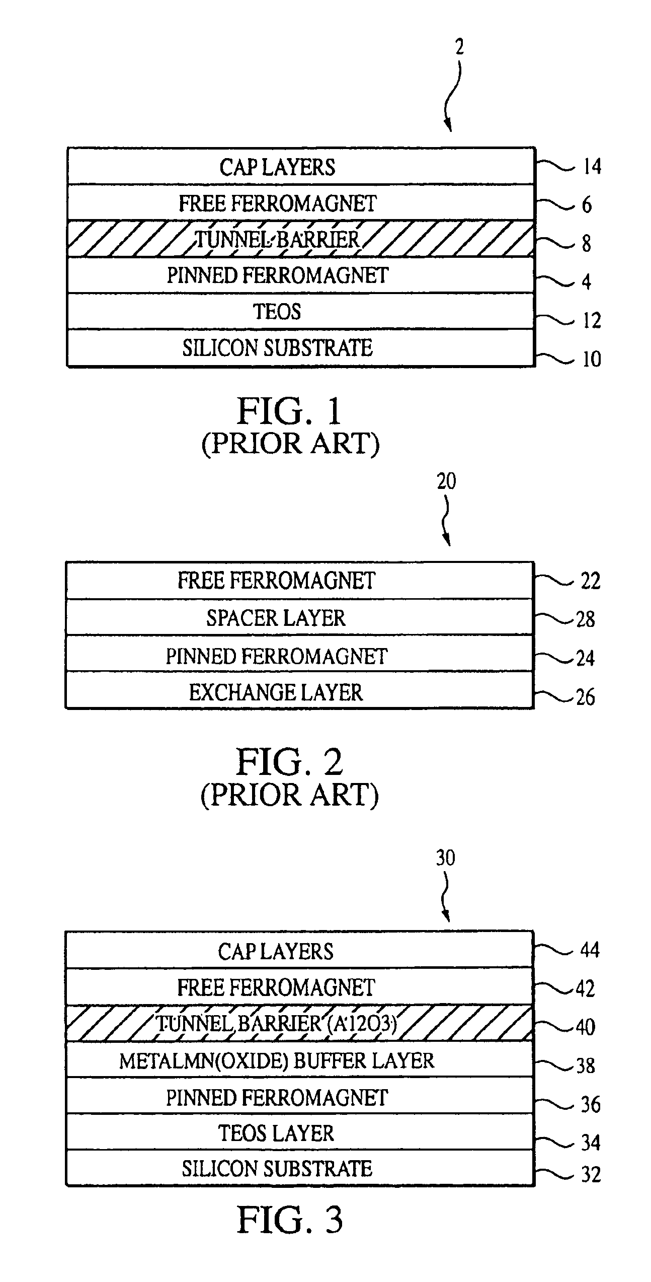
Referring to FIG. 3, a cross section is shown of an exemplary memory cell 30 constructed in accordance with an embodiment of the present invention. The memory cell 30 is formed over a substrate, for example, a silicon substrate 32. Insulating layers such as the illustrated TEOS layer 34 are formed over the substrate 32. A pinned ferromagnetic layer 36, typically formed of one or more layers of a ferromagnetic material and one or more layers of an anti-ferromagnetic material, is formed over the TEOS layer 34 and has a fixed magnetic orientation.

A metal manganese layer, such as FeMn (50:50), is deposited on the pinned ferromagnetic layer 36. FeMn layers can be deposited by sputtering, for example, or by other thin film fabrication techniques known in the art. Subsequent natural and / or assisted oxidation results in the formation of a metal manganese oxide (FeMnO) buffer layer 38.

The buffer layer 38 generally is formed of metal-manganese oxides or mixed metal-manganese oxides. The buffe...


PUM

PropertyMeasurementUnit
thicknessaaaaaaaaaa
thicknessaaaaaaaaaa
thickaaaaaaaaaa

Abstract

A metal manganese oxide buffer layer is used to seed a barrier layer in a magnetic tunnel junction memory element having pinned and free magnetic layers. An alumina tunnel barrier layer is formed on the oxidized metal manganese layer with the barrier layer and oxidized metal manganese layer being between the pinned or free ferromagnetic layers.

Description

BACKGROUND OF THE INVENTION1. Field of the InventionThe invention relates to magnetic film layers, and more specifically to providing smooth barrier layers in magnetoresistive devices.2. Brief Description of the Related ArtMagnetoresistive devices are known which take advantage of a magnetoresistive effect in electrically-conductive, multilayer structures containing ferromagnetic regions. The magnetoresistive effect is characterized by changes in electrical conductivity within the device due to the relative orientation of magnetic moments in the ferromagnetic regions. The magnetic orientation can be controlled by external fields, for example. Typically, the relative alignment of magnetic moments in the ferromagnetic regions can be parallel or antiparallel. Parallel alignment gives rise to one resistance in the device, whereas antiparallel alignment produces a different resistance. The different resistance values of the device can be translated into different logic signals.Examples o...

Claims


Application Information

Patent Timeline
Patent Type & Authority Patents(United States)
IPC IPC(8): B32B19/00G11B5/127H01L27/22H01L43/08H01L43/12
CPCH01L27/222H01L43/08H01L43/12Y10T428/12931Y10T428/32Y10T428/1193Y10T428/1114Y10T428/12465Y10T428/12611Y10T428/265H10B61/00H10N50/01H10N50/10
Inventor DREWES, JOEL A.
Owner MICRON TECH INC
Why Eureka
Try Eureka