Radiation correction method for electron beam lithography

a technology radiation correction method, which is applied in the direction of photomechanical treatment originals, photomechanical instruments, photomechanical apparatus, etc., can solve the problems of inconvenient operation, inconvenient operation, and inability to solve the problem of electron beam lithography radiation correction method, etc., and achieve the effect of being ready for commercialization

Inactive Publication Date: 2005-03-29
TAIWAN SEMICON MFG CO LTD
View PDF7 Cites 25 Cited by
  • Summary
  • Abstract
  • Description
  • Claims
  • Application Information

AI Technical Summary

Benefits of technology

[0026]The present invention employs methods and materials for pattern generation and fabrication as are known in the art of microelectronics fabrication, but in a novel order and arrangement. The method of the invention is therefore readily commercially implemented.

Problems solved by technology

In the early stages of development of microelectronics fabrication technology, such master image patterns were generally enlarged versions of the pattern which were then reduced by photographic methods to the final dimensions on the working photomask This process was tedious and costly, and has been largely replaced by the use of direct exposure of the photomask opaque blank substrate, coated with a layer of sensitive resist material, to the desired pattern.
Although effective for many purposes, this dose correction method is not without problems, particularly with respect to being costly and time-consuming.
Although the method of dose correction of the written pattern or the “ghost” correction method are in general satisfactory for general use in electron beam lithography, neither method is entirely without problems.
Densely populated patterns require inordinately long and costly calculation of incremental dose correction adjustments for each pattern element in the dose correction method.
For small features and / or sparsely populated designs, the time required for the second exposure of the “ghost” correction method is time consuming and the defocused beam may cause resolution problems.

Method used


Image

  • Radiation correction method for electron beam lithography
  • Radiation correction method for electron beam lithography
  • Radiation correction method for electron beam lithography

Examples


first preferred embodiment

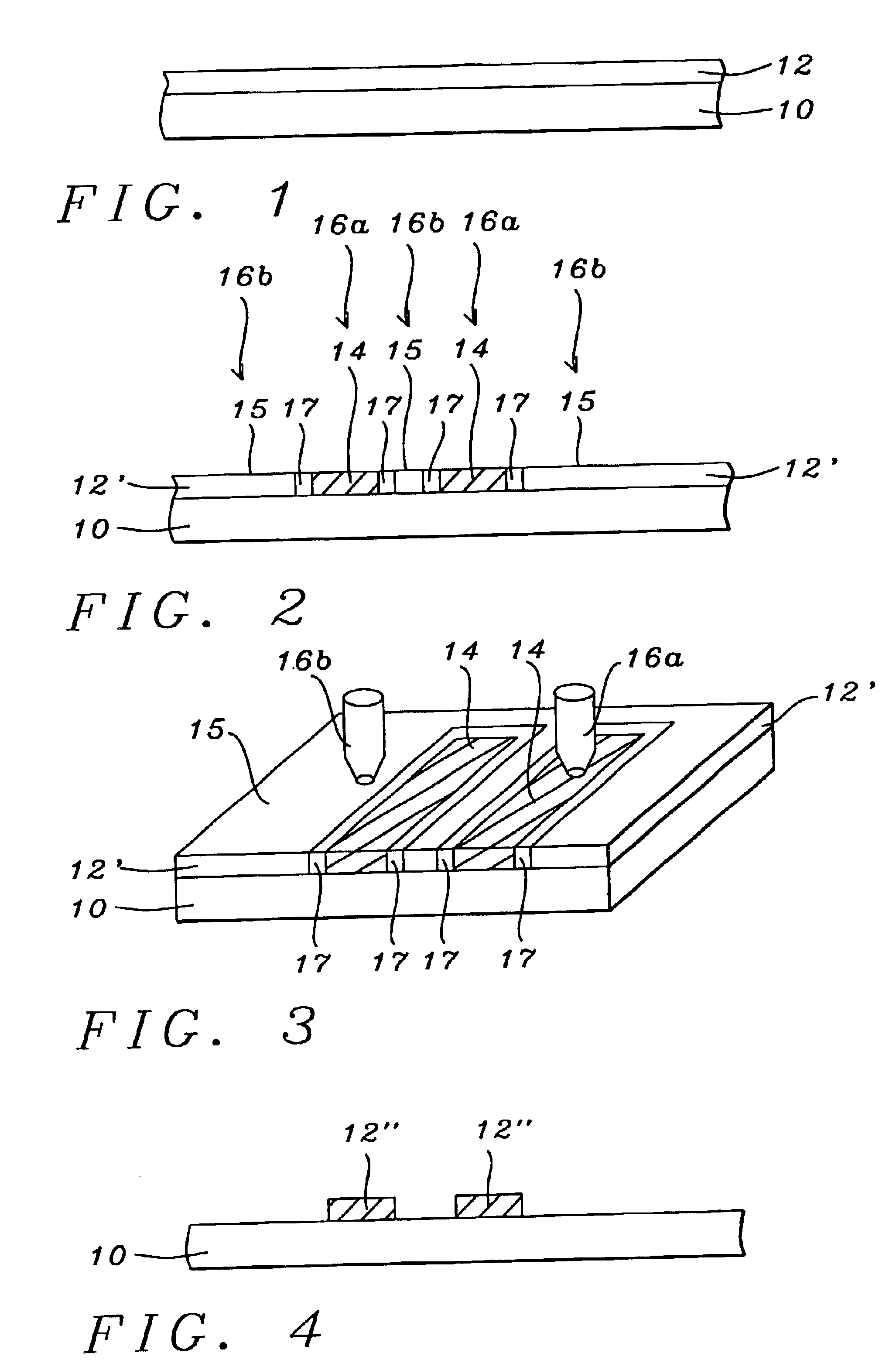
[0033]FIG. 1 to FIG. 5 are a series of schematic diagrams illustrating the results of forming upon a substrate a patterned resist layer by vector scan electron beam exposure with optimal proximity effect exposure dose correction and “ghost” pattern correction with a shaped focused beam FIGS. 1-2 and FIGS. 4-5 are schematic cross-sectional diagrams illustrating progressive stages in the fabrication of the patterned resist layer; FIG. 3 is a schematic plan view of the patterned resist layer corresponding to FIG. 2. FIG. 1 is a schematic cross-sectional diagram of the substrate at an early a stage in its fabrication in accord with a first preferred embodiment of the present invention.

[0034]Shown in FIG. 1 is a substrate 10 having formed thereupon a sensitive resist layer 12.

[0035]With respect to the substrate 10 shown in FIG. 1, the substrate 10 is formed employing material selected from the group consisting of microelectronics conductor materials, microelectronics semiconductor materi...

second preferred embodiment

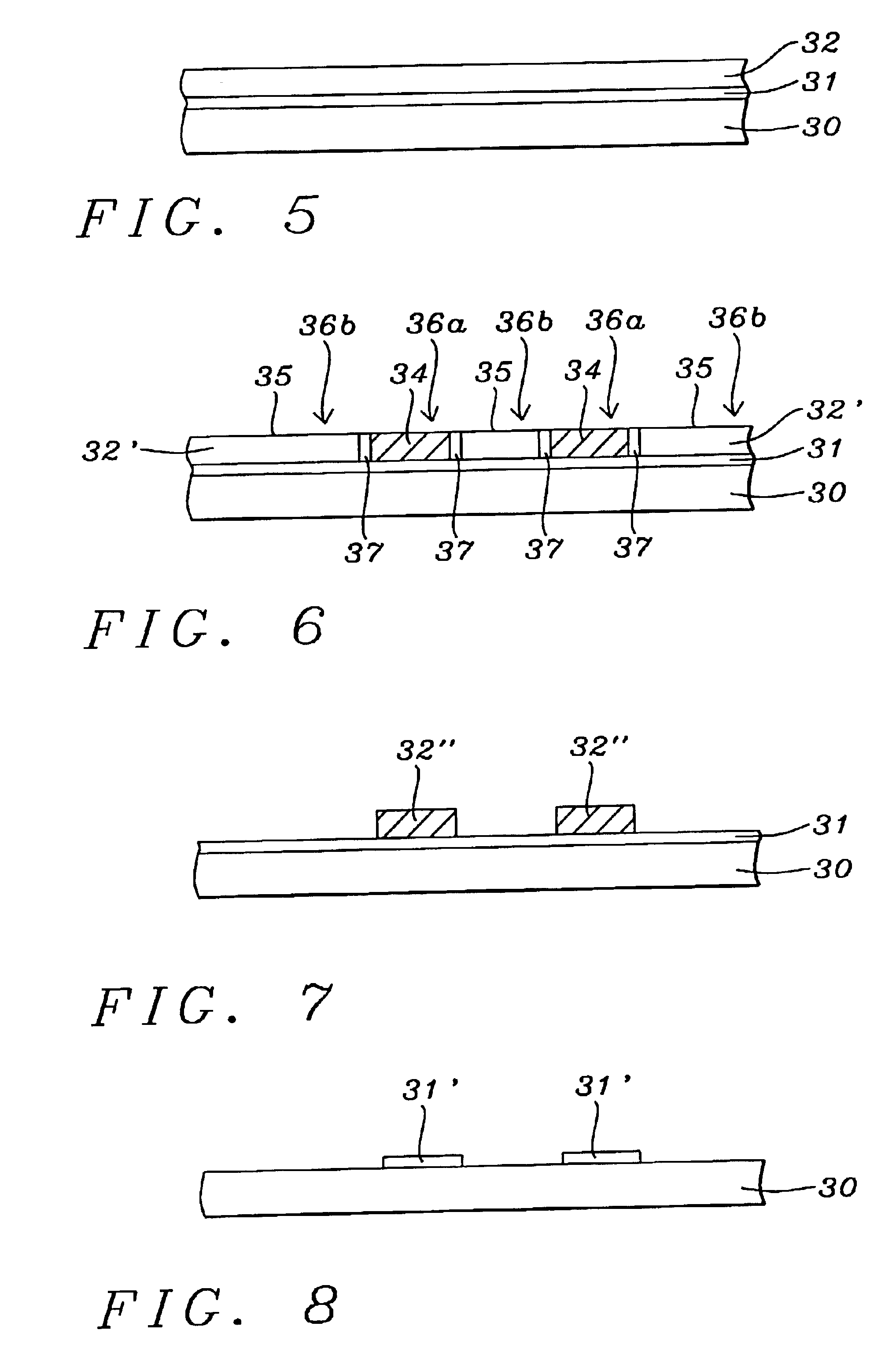
[0042]Referring now more particularly to FIG. 5 to FIG. 8, FIG. 5 to FIG. 8 show a series of schematic cross-sectional diagrams illustrating the results of forming a patterned photomask employing electron beam lithography of an electron beam resist material with optimal correction for proximity effects due to electron back scattering into the resist layer. FIG. 5 is a schematic cross-sectional diagram of a photomask substrate at an early stage in its fabrication in accord with a more specific embodiment of the present invention which constituted a second preferred embodiment of the present invention. Shown in FIG. 5 is a photomask substrate 30 over which is formed an opaque layer 31 and a sensitive resist layer 32.

[0043]With respect to the photomask substrate 30 shown in FIG. 5, the photomask substrate 30 is analogous to the substrate 10 shown in FIG. 1 of the first embodiment of the present invention, and is formed of transparent material. Preferably the substrate 30 is formed of o...


PUM

PropertyMeasurementUnit
phase angleaaaaaaaaaa
widthaaaaaaaaaa

Abstract

A method for forming a patterned microelectronics layer employing electron beam lithography in a sensitive material upon a substrate with optimal correction for proximity effects resulting from electron back scattering into the resist material. There is provided a substrate having formed thereon a layer of resist material sensitive to electron beam exposure. There is then exposed the sensitive layer to a vector scan shaped electron beam to write a primary pattern with dose correction of the beam dose for proximity effects due to electron scattering at each point in the primary pattern. There is then written a secondary pattern which is a negative reversed image of the primary pattern in a secondary exposure employing a vector scan shaped focused electron beam at an exposure dose substantially below the primary beam dose, there being provided a gap between the primary pattern and the secondary pattern. There is then developed the primary pattern in the sensitive resist layer to form the final corrected pattern on the substrate. The patterned layer of resist material may be employed directly on the substrate on which it is formed, or alternatively the patterned resist layer may be employed formed over an opaque layer upon the transparent substrate and subsequently the pattern etched into the opaque layer to form a photomask.

Description

BACKGROUND OF THE INVENTION[0002]1. Field of the Invention[0003]The invention relates to the field of manufacture of microelectronics devices employing patterned etch mask resist layers to form patterns. More particularly the invention relates to the employment of electron beam microlithography fabrication methods to form patterned etch resist mask layers and patterned photomasks.[0004]2. Description of the Related Art[0005]Microelectronics fabrications consist of multiple layers of microelectronics materials formed on a substrate. Many of the microelectronics layers are patterned and must be not only accurate and precise in themselves, but must also be registered with great precision to other patterned layers. These objectives are met by employing photolithographic methods in which the desired patterns are first formed as patterned stencil photomasks with opaque and transparent regions. This pattern is then transferred to a photosensitive layer or photoresist by illumination throug...

Claims


Application Information

Patent Timeline
Patent Type & Authority Patents(United States)
IPC IPC(8): G03F9/00G03C5/00G03F7/20H01J37/302
CPCG03F1/78G03F7/2061H01J37/3026G03F7/2063Y10S430/143H01J2237/31771
Inventor TZU, SAN-DECHIU, CHING SHIUNCHOU, WEI-ZENWU, CHIA FANG
Owner TAIWAN SEMICON MFG CO LTD
Why Eureka
Try Eureka