Wiring board provided with passive element and cone shaped bumps

a technology of passive elements and wiring boards, which is applied in the direction of printed element electric connection formation, magnets, magnetic bodies, etc., can solve the problems of low design allowance when the passive elements are arranged, inability to obtain a smaller size, and warpage of multi-layered substrates, etc., and achieve excellent characteristics.

Inactive Publication Date: 2005-03-29
DAI NIPPON PRINTING CO LTD
View PDF30 Cites 60 Cited by
  • Summary
  • Abstract
  • Description
  • Claims
  • Application Information

AI Technical Summary

Benefits of technology

That is, a resistive paste is coated on a metal foil. Accordingly, the heat-treatment (such as, for instance, drying, sintering, and curing) and so on of the paste can be performed irrespective of the heat resistance temperature of an insulating board. Thereafter, the metal foil having thus, for instance, heat-treated paste (resistive element) and the insulating board are laminated. Accordingly, a wiring board provided with passive elements (resistors in this case) having excellent characteristics can be obtained.
Furthermore, in this case, the wiring board may be configured so that the conductive bump may directly establish one or both of an electrical contact and a heat conductive contact with the coated/formed res...

Problems solved by technology

However, in this technique, the multi-layered substrate may warp due to the difference of characteristics such as thermal expansion coefficient and so on between the substrate materials.
In addition, since only one specified kind of passive element may be formed in one layer, a design allowance when the passive elements are arranged is low.
That is, it is inappropriate in obtaining a smaller size due to tendency to an increase in the number of layers as a whole.
Furt...

Method used


Image

  • Wiring board provided with passive element and cone shaped bumps
  • Wiring board provided with passive element and cone shaped bumps
  • Wiring board provided with passive element and cone shaped bumps

Examples


Embodiment Construction

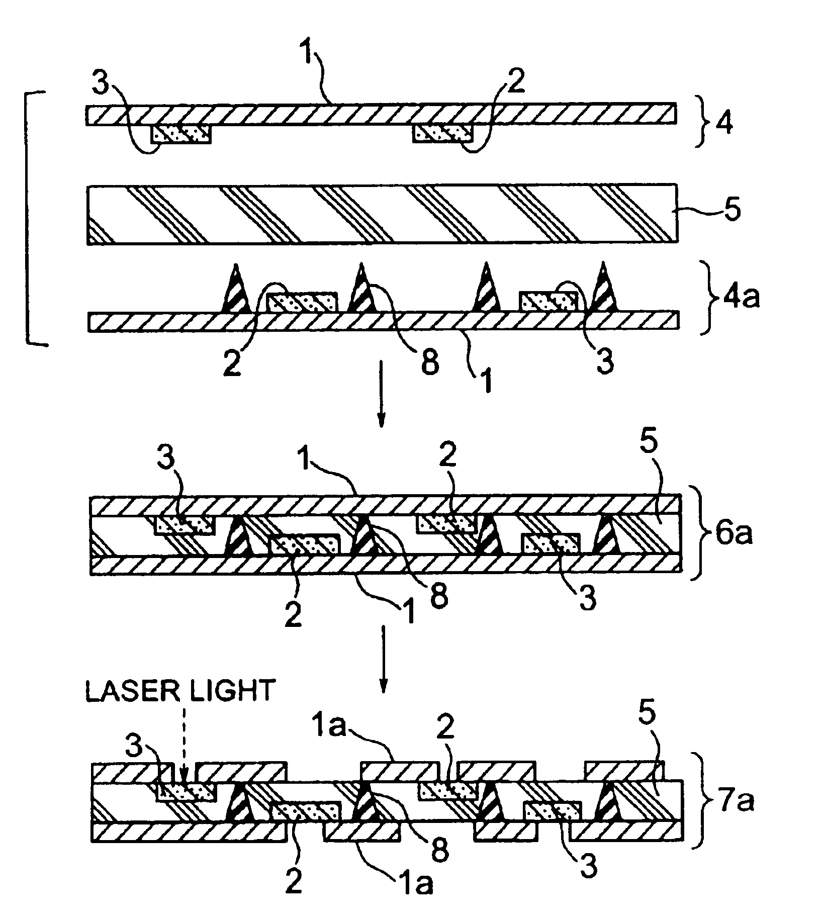
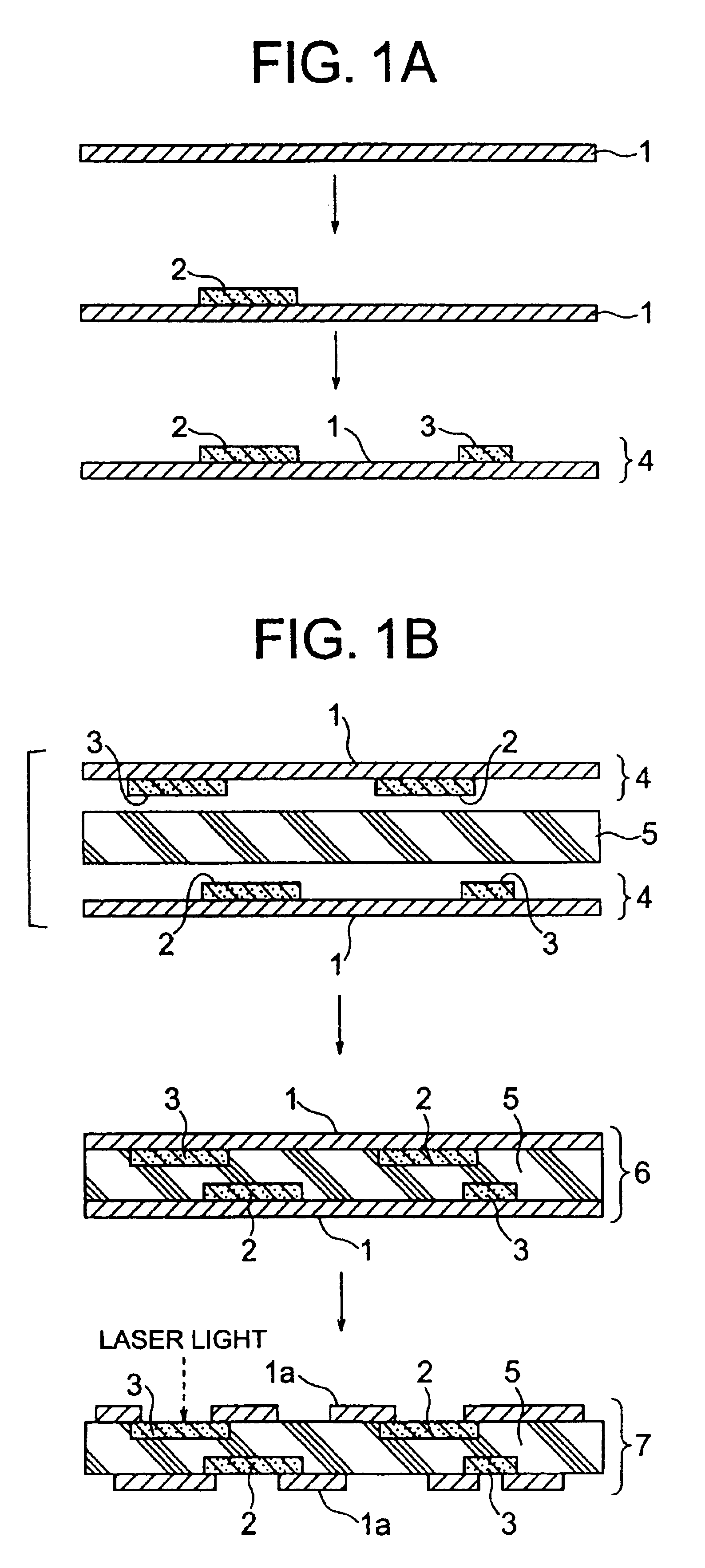
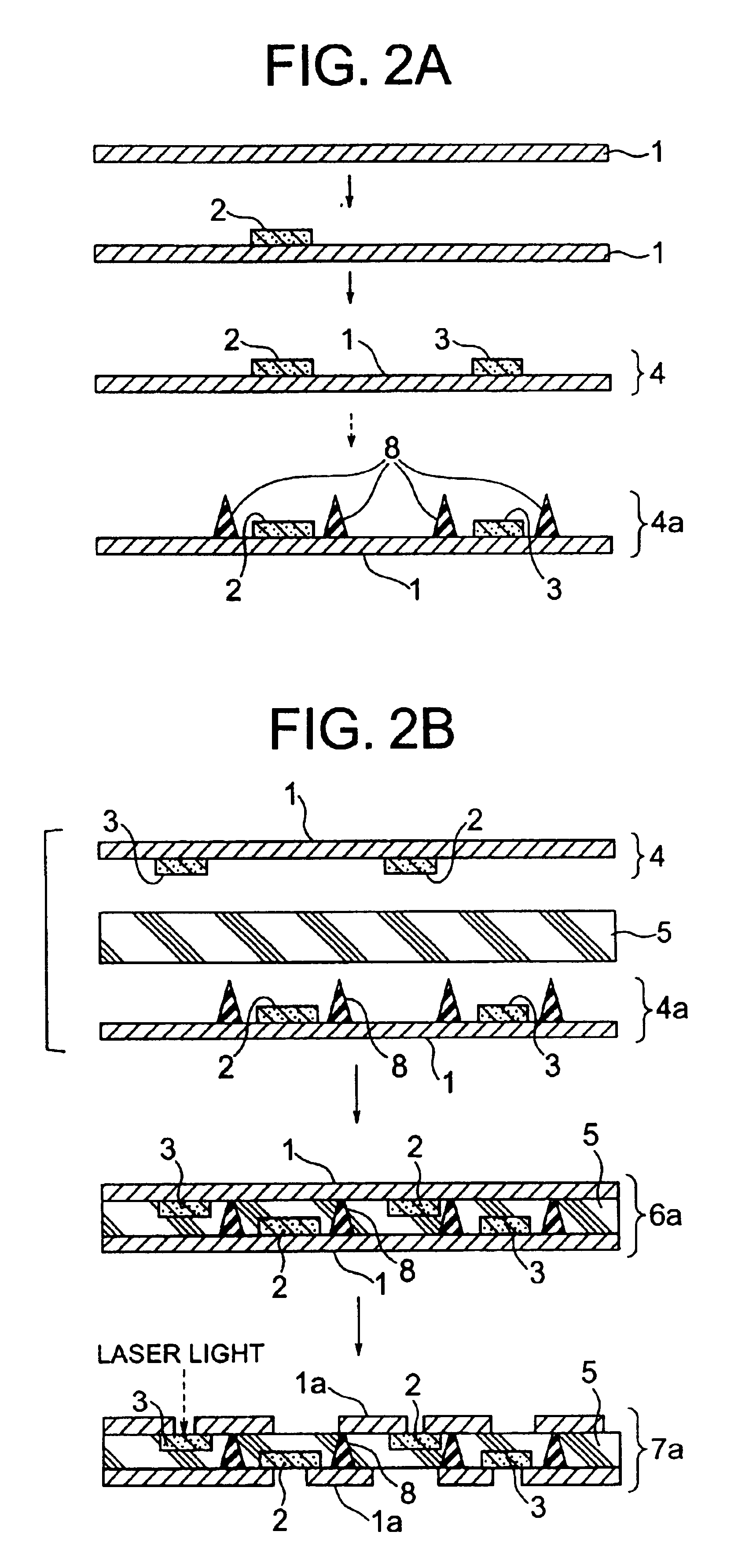
The fabricating method according to the present invention, as an implementation mode, further includes forming a substantially conical conductive bump on the first surface of the first metal foil. In this case, the forming a double-sided wiring board is performed so that the formed conductive bump may penetrate through the insulating board and establish an electrical contact with the second metal foil. That is, since wiring layers on both sides are electrically connected by means of a conductive bump, the number of the processes may be reduced and a double-sided wiring board whose wiring layers on both sides have an electrical continuity may be easily fabricated.

Furthermore, in an implementation mode of the fabricating method according to the present invention, the patterning the first metal foil and / or the second metal foil includes the formation of an inductor that is vortically formed due to a pattern and / or a loop antenna that is formed loop-like due to a pattern. That is, an in...


PUM

PropertyMeasurementUnit
Thicknessaaaaaaaaaa

Abstract

A fabricating method of a wiring board provided with passive elements is disclosed. The fabricating method includes coating one or both of resistive paste and dielectric paste on at least any one of first surfaces of a first metal foil and a second metal foil each of which has a first surface and a second surface; arranging an insulating board having thermo-plasticity and thermo-setting properties so as to face the first surface of the first metal foil, and arranging the first surface side of the second metal foil so as to face a surface different from a surface to which the first metal foil faces of the insulating board; forming a double-sided wiring board by stacking, pressurizing and heating the arranged first metal foil, insulating board, and second metal foil, and thereby integrating these; and patterning the first metal foil and/or the second metal foil.

Description

BACKGROUND OF THE INVENTION1. Field of the InventionThe present invention relates to a method for fabricating a wiring board provided with a passive element and to a wiring board provided with a passive element, in particular to a method for fabricating a wiring board provided with a passive element having an aptitude for improving characteristics of the passive element and to a wiring board provided with a passive element having an aptitude for improving characteristics of the passive element.2. Description of the Related ArtAs portable electronic devices become smaller in size, lighter in weight and thinner in thickness, smaller size chip components, such as L (inductor, coil), C (condenser, capacitor) and R (resistor), have been developed. Furthermore, by burying passive elements such as C and L in a wiring substrate, composite components have been developed. Such integration with a wiring substrate has been actively forwarded particularly in multi-layered ceramic substrates and ...

Claims


Application Information

Patent Timeline
IPC IPC(8): H05K1/16H05K3/40H05K3/46H05K1/09
CPCH05K1/165H05K1/167H05K1/162H05K1/095Y10T29/4902H05K3/4069H05K3/4614H05K3/4652H05K2201/0187H05K2201/0355H05K2201/086H05K2201/09763H05K2203/0338H05K2203/1189Y10T29/49128Y10T29/49126Y10T29/49117Y10T29/49099Y10T29/49155
Inventor FUKUOKA, YOSHITAKASERIZAWA, TOORUYAGI, HIROSHISHIMADA, OSAMUHIRAI, HIROYUKIYAMAGUCHI, YUJI
Owner DAI NIPPON PRINTING CO LTD
Why Eureka
Try Eureka