Display device and driving method thereof

a technology of display device and driving circuit, which is applied in the field of display device, can solve the problems of short interval between battery charging of mobile instruments, increase in cost, and complicated structure of driving circuit, and achieve the effect of reducing power consumption and the size of display devi

Inactive Publication Date: 2005-03-29
KK TOSHIBA
View PDF7 Cites 80 Cited by
  • Summary
  • Abstract
  • Description
  • Claims
  • Application Information

AI Technical Summary

Benefits of technology

In view of the above-described problems, it is an object of the present invention to provide a display device which can reduce power consumption and size of the display device.

Problems solved by technology

Since power consumption in the color display device is larger than that in the monochrome display device, the color display device has a problem that an interval of battery charging of the mobile instrument is short.
Furthermore, since a circuit is also complicated, miniaturization is difficult, which leads to increase in cost.
In case of the color display device, however, not only the structure of the driving circuit is complicated, but a capacity of a memory storing therein pixel data is also increased.
Therefore, it is technically difficult to integrally form the driving circuit on the pixel array substrate.
In such control in accordance with each horizontal pixel line, however, the low-consumption power is not necessarily attained as compared with control at the time of usual driving.

Method used


Image

  • Display device and driving method thereof
  • Display device and driving method thereof
  • Display device and driving method thereof

Examples


first embodiment

(First Embodiment)

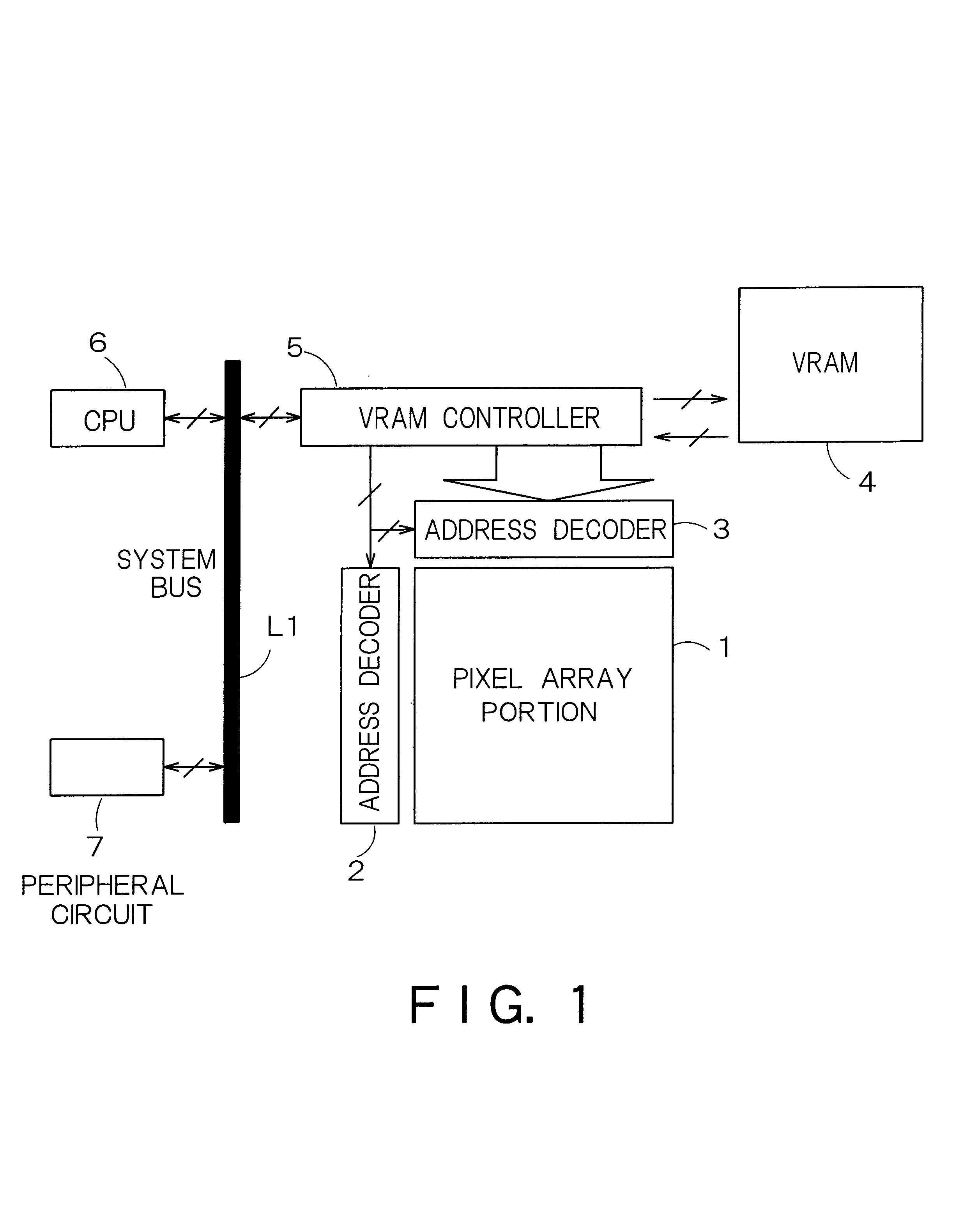
FIG. 1 is a block diagram showing a schematic configuration of a first embodiment of a display device according to the present invention, and illustrates a structure of a liquid crystal display.

The liquid crystal display shown in FIG. 1 includes a pixel array portion 1, address decoders 2 and 3, a display memory (VRAM) 4, and a VRAM controller 5, and transmits / receives signals to / from a CPU 6 and a peripheral circuit 7 through a system bus L1.

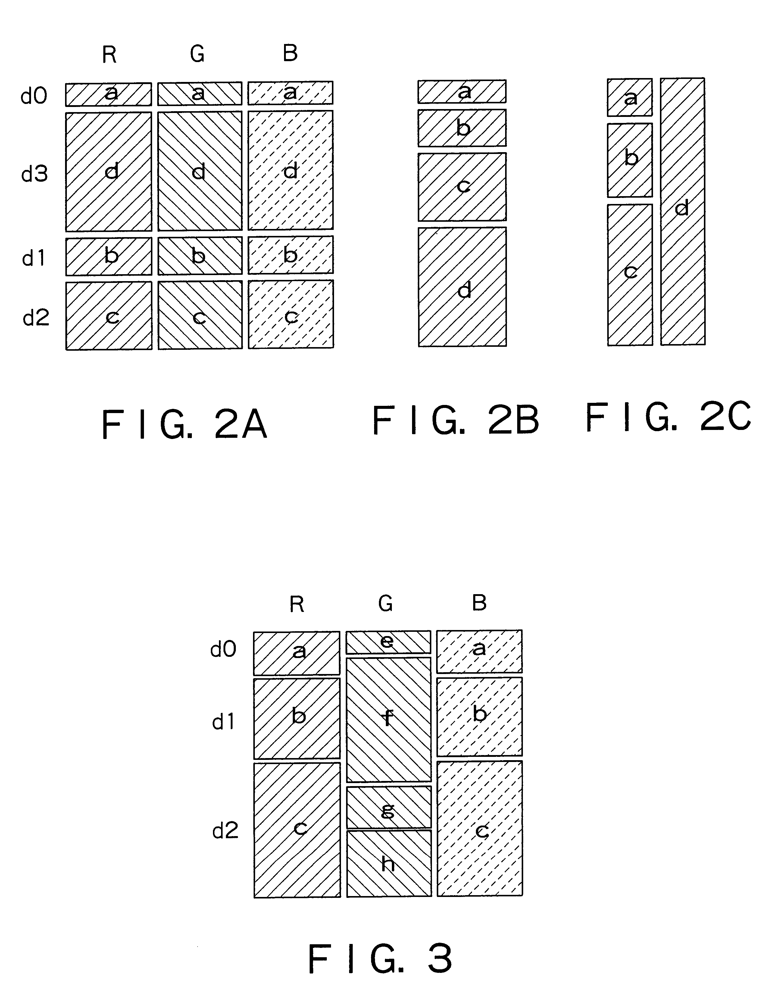
The pixel array portion 1 has a pixel structure capable of performing area gradation display in which each pixel is composed of a plurality of one-bit memories. FIGS. 2A, 2B and 2C are views showing each structure corresponding to one pixel. As shown in the drawings, one pixel is composed of four sub pixel areas in accordance with each color display pixel of RGB, and a memory for one bit is provided to each area. FIGS. 2A and 2C show examples in which one display pixel is composed of four sub pixel areas based on a display sig...

specific example 1

of Memory and Polarity Inverting Circuit

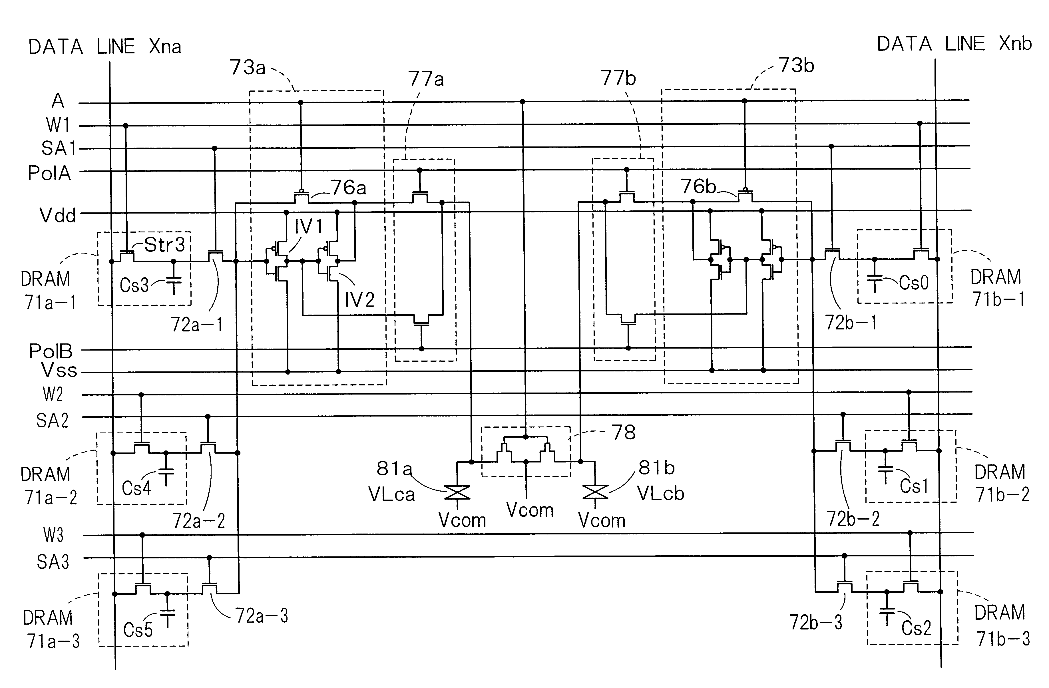
FIG. 6 is a circuit diagram showing configuration of a liquid crystal display in which an SRAM and a polarity inverting circuit are provided in accordance with each sub pixel having a weighted display area. Parts surrounded by dashed lines in FIG. 6 indicate respective sub pixels. To each sub pixel are connected a word line, polarity control lines P+ and P− and a data line, and each sub pixel has a single-word line structure. Each sub pixel has a transistor Q3 which is turned on / off by a potential of the word line, a transistor Q4 which is turned on / off by a potential of the polarity control line P+, a transistor Q5 which is turned on / off by a potential of the polarity control line P−, and inverters IV3 and IV4 connected in cascade. The transistor Q3 and the inverters IV3 and IV4 constitute an SRAM, and the transistors Q4 and Q5 form a polarity inverting circuit.

The circuit of FIG. 6 is relatively simple. By combining random access circuits fo...

specific example 2

of Memory and Polarity Inverting Circuit

FIG. 7 is a circuit diagram of a double-word line structure. The circuit shown in FIG. 7 has a transistor Q6 which is turned on / off by the potential of a column word line. When the transistor Q6 is turned on, the potential of the main word line is supplied to the sub word line. The sub word line is connected to each of the sub pixels aligned in the row direction. For example, when the sub word line is on the high level, a transistor Q3 is turned on, and a transistor Q7 provided in a feedback path of the SRAM is turned off. At this moment, either the transistor Q4 or Q5 is turned on by the potential of the polarity control lines P+ and P−.

On the other hand, when the sub word line is on the low level, the transistor Q7 is turned on, and an inverter output on the rear stage side in the SRAM is fed back to the input of the inverter on the first stage side, thereby holding data.

As described above, in the double word line structure, the sub word lin...


PUM

PropertyMeasurementUnit
threshold voltageaaaaaaaaaa
voltagesaaaaaaaaaa
ground voltage VSSaaaaaaaaaa

Abstract

A liquid crystal display device which can reduce power consumption and can be miniaturized. The liquid crystal display device according to the present invention includes a pixel array portion, an address decoder, a display memory (VRAM), and a VRAM controller, and transmits / receives a signal to / from a CPU and a peripheral circuit through a system bus. The pixel array portion has an area gradation pixel structure in which each pixel is composed of a plurality of one-bit memories. The entire pixel array portion is divided into pixel blocks each of which consists of a plurality of pixels, and the one-bit memory is rewritten in units of block. The one-bit memory has a double-word line structure.

Description

CROSS REFERENCE TO RELATED APPLICATIONSThis application is based upon and claims the benefit of priority from the prior Japanese Patent Applications No. 2000-269177, filed on Sep. 5, 2000, the entire contents of which are incorporated herein by reference.BACKGROUND OF THE INVENTION1. Field of the InventionThe present invention relates to a display device, and more specifically, it relates to a technique for reducing power consumption and simplifying a circuit configuration.2. Related Background ArtMonochrome display devices were often provided in conventional mobile instruments such as mobile phones. Recently, with increase of opportunities such as connections to an Internet using the mobile instruments, the mobile instruments having color display devices has increased.Since power consumption in the color display device is larger than that in the monochrome display device, the color display device has a problem that an interval of battery charging of the mobile instrument is short. ...

Claims


Application Information

Patent Timeline
Patent Type & Authority Patents(United States)
IPC IPC(8): G09G3/36G09G3/32G02F1/133G09G3/20
CPCG09G3/3618G09G3/3666G09G3/2022G09G3/2074G09G3/32G09G3/3614G09G2330/021G09G2300/0452G09G2300/0828G09G2300/0842G09G2300/0857G02F1/133
Inventor NAKAMURA, TAKASHI
Owner KK TOSHIBA
Why Eureka
Try Eureka