Unbuffered memory system

a memory system and buffer technology, applied in the field of memory systems, can solve the problems of adverse effects on the propagation of high-frequency c/a signals, and achieve the effect of excellent waveform characteristics

Inactive Publication Date: 2005-03-29
LONGITUDE LICENSING LTD
View PDF3 Cites 6 Cited by
  • Summary
  • Abstract
  • Description
  • Claims
  • Application Information

AI Technical Summary

Benefits of technology

As a result of carrying out a simulation and repeating consideration for solving the foregoing problems, the inventors of the present invention have found in the course thereof that, particularly in case of a memory module with ECC function, excellent waveform propagation can be achieved by employing a single T-branch topology as an internal C / A bus topology, rather than a dual T-branch topology. This means that from an aspect of wiring layout, a more simplified wiring layout can be employed.
It is also concluded that it is effective to connect a capacitor to a signal bus connecting between the memory controller and the memory module for cutting high-frequency components of a C / A signal propagating on the signal bus. Specifically, by connecting one end of the capacitor to the signal bus and feeding the fixed potential (e.g. ground potential) to the other end thereof, noise in a broad sense can be reduced, thereby to achieve an excellent waveform characteristic.
In the foregoing unbuffered memory systems, the memory devices may be disposed evenly or unevenly on right and left sides with respect to the branch point on the module wiring. For example, if the number of the mounted memory devices is one of 4, 8 and 16, the memory devices may be arranged evenly, while, if the number of the mounted memory devices is one of 5, 9 and 18, the memory devices may be arranged unevenly. The configuration of each of the foregoing unbuffered memory systems significantly contributes to excellent waveform characteristics particularly when the operating frequency of a C / A signal exceeds 100 MHz, but may be operated at the frequencies equal to or below 100 MHz. In the foregoing unbuffered memory systems, the wiring impedance of the module wiring is preferably within the range of 50Ω to 65Ω.

Problems solved by technology

For example, a MOS transistor is normally provided as an output transistor in an output stage of a memory controller and, if the MOS transistor is operated in a region other than a region (linear region in VD-ID characteristic of MOS transistor) where the on-resistance of the MOS transistor becomes substantially constant, high-frequency C / A signal propagation is adversely affected.

Method used


Image

  • Unbuffered memory system
  • Unbuffered memory system
  • Unbuffered memory system

Examples


first embodiment

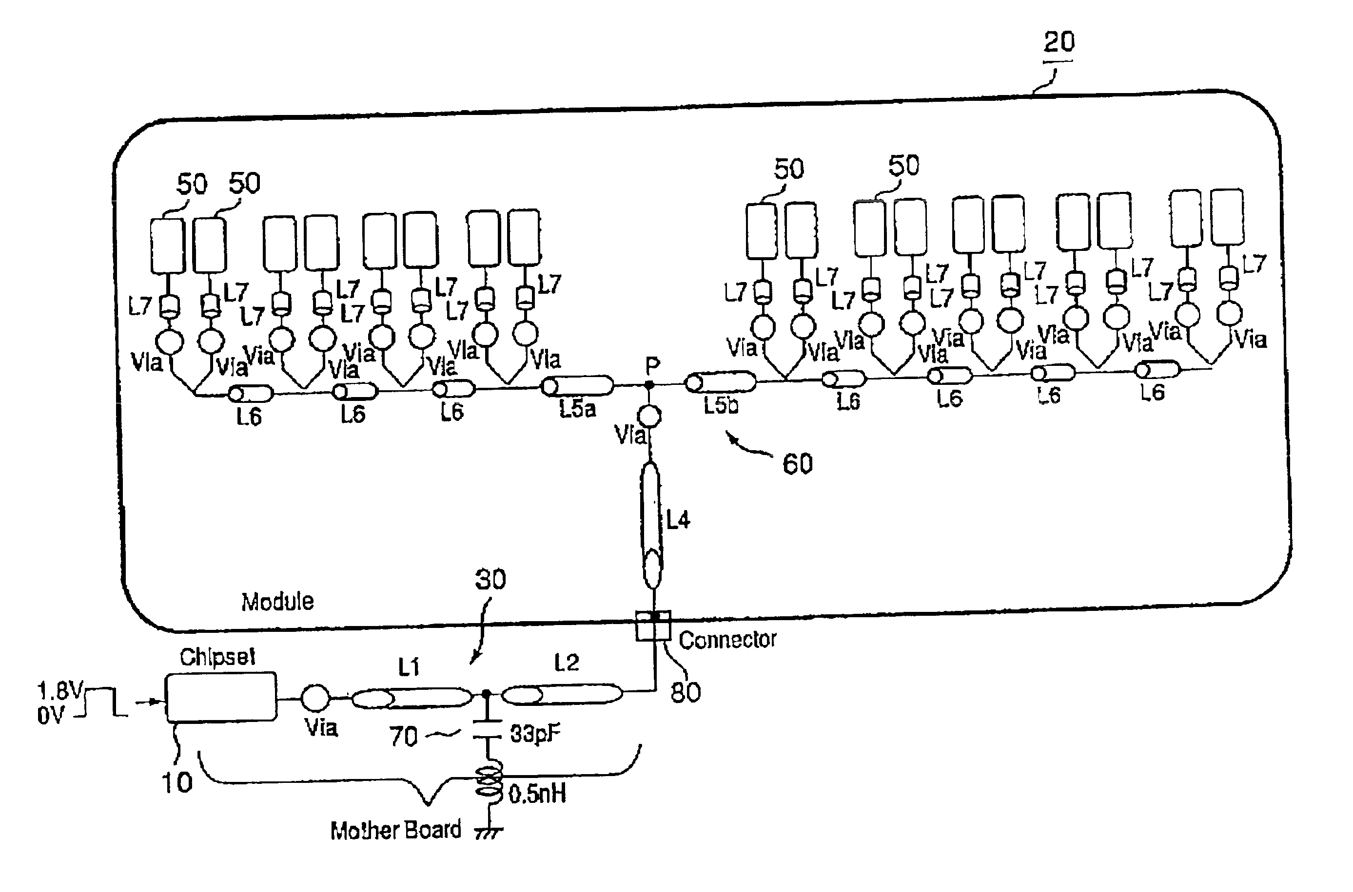
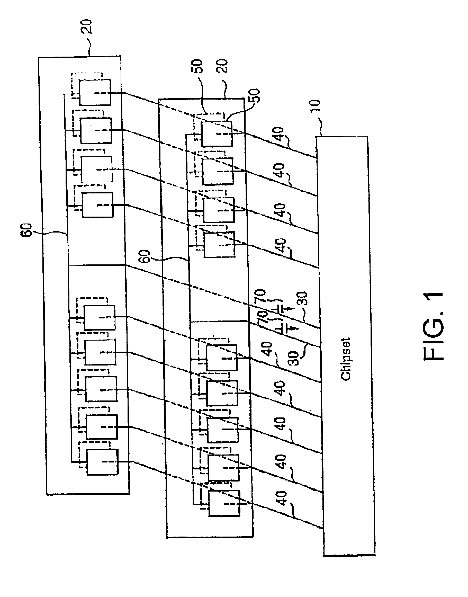
As shown in FIG. 1, a memory system according to the first embodiment of the present invention comprises a chipset 10, memory modules 20, C / A buses 30 and CLK buses 40. On each of the memory modules 20 in this embodiment, a total of 18 DRAM devices 50 are mounted, with 9 DRAM devices 50 on each side thereof. The DRAM devices 50 all have the same characteristics, and the memory module 20 is assumed to have an ECC function.

Inasmuch as FIG. 1 conceptually shows the memory system according to this embodiment, a mother board is omitted. In the actual system, however, the chipset 10 is mounted on a mother board, and the C / A buses 30 and the CLK buses 40 are also disposed on the mother board. A capacitor 70 is connected to each C / A bus 30. Further, sockets are provided on the mother board and, by inserting a connector, which will be described later, of the memory module 20 into each of the sockets, the memory system shown in FIG. 1 is constituted. Specifically, by the insertion of the memo...

second embodiment

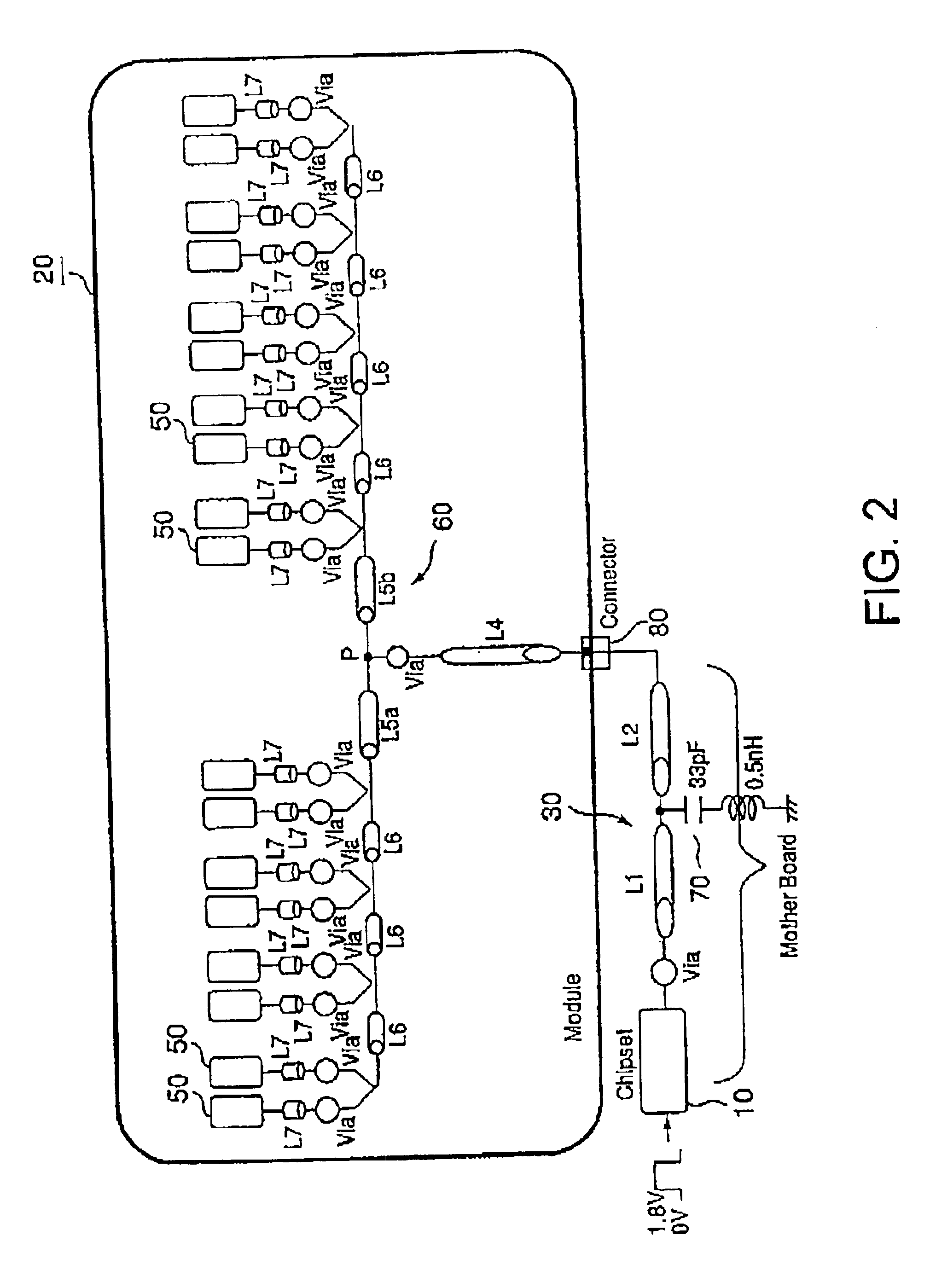
A memory system according to the second embodiment of the present invention is a modification of the foregoing first embodiment. In such a modification, the number of the devices mounted on a memory module 20 is set to 9.

The memory system according to the second embodiment shown in FIG. 14 differs from the first embodiment in that, other than the mounted device number, a terminating resistor 90 is added to an internal C / A bus 60. This is adopted as a countermeasure because overshoot is caused following the reduction in mounted device number. The other configuration such as a configuration of a chipset 10, an equivalent circuit of a connector 80, an equivalent circuit of a via hole, an equivalent circuit of a DRAM device 50 and so on are like those in the first embodiment, and thus explanation thereof will be omitted hereinbelow. Further, since things related to the output impedance of the chipset 10 are also like in the foregoing first embodiment, explanation thereof will also be om...

third embodiment

Like the second embodiment, a memory system according to the third embodiment of the present invention is provided with a countermeasure for overshoot that is caused by setting the mounted device number to nine.

In the overshoot countermeasure according to this embodiment, a resistor having a predetermined value is inserted on the first wiring portion of the internal C / A bus 60 (i.e. between the connector 80 and the branch point P). Specifically, as shown in FIG. 16, a resistor 100 having a resistance value Rs (=10Ω±20%) is connected in series between the wiring L4 and the branch point P.

With this structure, in addition to the effect achieved by the second embodiment, the overshoot level can be further lowered and, since the power for operating the terminating resistor is not required, the power saving can be accomplished.


PUM


Abstract

A memory module of the unbuffered type with ECC function is employed. Configuration of an internal C / A bus is set to a single T-branch topology. An output impedance of a chipset is maintained substantially constant. A capacitor for cutting high-frequency components of a C / A signal is added on a C / A bus.

Description

BACKGROUND OF THE INVENTION1. Field of the InventionThe present invention relates to a memory system having a memory module and, in particular, relates to a memory system having, as a memory module, an unbuffered memory module with no buffer or register.2. Description of the Related ArtIn general, memory systems each comprise a memory module mounted thereon with memory devices, a memory controller for outputting information necessary for operations of the memory devices mounted on the memory module, i.e. command / address (C / A) signals, input data signals and so on, and a signal bus connecting between the memory controller and the memory module. For example, when the memory module is used as a main memory in a computer system, the memory controller is in the form of a chipset or the like and the signal bus is in the form of wirings extended on a mother board.Among them, the memory modules are roughly classified into memory modules with registers (or memory modules with buffers) and un...

Claims


Application Information

Patent Timeline
Patent Type & Authority Patents(United States)
IPC IPC(8): G06F12/00G06F13/16G06F9/26G11C5/02G06F12/06G06F13/40G11C5/00G11C5/06G11C7/10
CPCG06F13/4086G11C7/1078G11C5/063G11C5/04
Inventor SHIBATA, KAYOKONISHIO, YOJI
Owner LONGITUDE LICENSING LTD
Why Eureka
Try Eureka