Electrochemical assisted CMP

a technology of electrochemical assisted and substrate, which is applied in the direction of electrolysis components, manufacturing tools, lapping machines, etc., can solve the problems of reducing the feature size, reducing the service life of the substrate, so as to reduce the application force, reduce the stress, and reduce the effect of tearing and fractur

Inactive Publication Date: 2005-04-05
APPLIED MATERIALS INC
View PDF19 Cites 12 Cited by
  • Summary
  • Abstract
  • Description
  • Claims
  • Application Information

AI Technical Summary

Benefits of technology

dvantages. One notable benefit and advantage of the invention is by minimizing the shear stresses realized at the surface of the substrate during processing, the process is ideally suited for fragile, porous low-k dielectric films with copper metallization. The downforces exerted during processing remain less than 1 psi, and so tearing and fracture notably associated with porous and highly porous low-k dielectrics is minimized or eliminated.
Another benefit is economy and efficiency of implementation. With the growing use of electroplating methods and apparatus to deposit conductive fill in smaller and smaller feature sizes, embodiments of the present invention implement similar processes that can be realized with minimal modification of existing apparatus. Both CMP and electroplating are known and used processes, making necessary and desired components of the present invention readily accessible.
An additional benefit is the ability to achieve desired control of the removal to meet stringent requirements within exacting tolerances of next generation processes. In conventional CMP processes, minimizing applied forces yields unacceptably low removal rates, reduced productivity, and increased cost of production. Embodiments of the present invention provide for minimal force application with sufficient removal rate combined with the necessary control of the process in the small feature environment.
Other advantages of the invention will become apparent from the following detailed description, taken in conjunction with the accompanying drawings, illustrating by way of example the principles of the invention.

Problems solved by technology

The processing forces result in significant shear stress on the surface of the substrate being planarized or otherwise processed.
The porous, low-k dielectric material which serves as an insulating material for the copper or other metal wiring is fragile, and particularly susceptible to fracture and tearing under applied shear stress.
In addition to the fragile, porous low-k dielectric material, fabrication challenges also include progressively smaller feature sizes.
Electropolish processes for the removal of copper or other metal overburden, and for planarization of a substrate, are generally deficient with respect to stringent overburden removal and planarization requirements.
Electropolish material removal is intrinsically isotropic, and is unable to be implemented for selective removal of hundreds or a few thousands of angstroms (Å) of topography.

Method used


Image

  • Electrochemical assisted CMP
  • Electrochemical assisted CMP
  • Electrochemical assisted CMP

Examples


Embodiment Construction

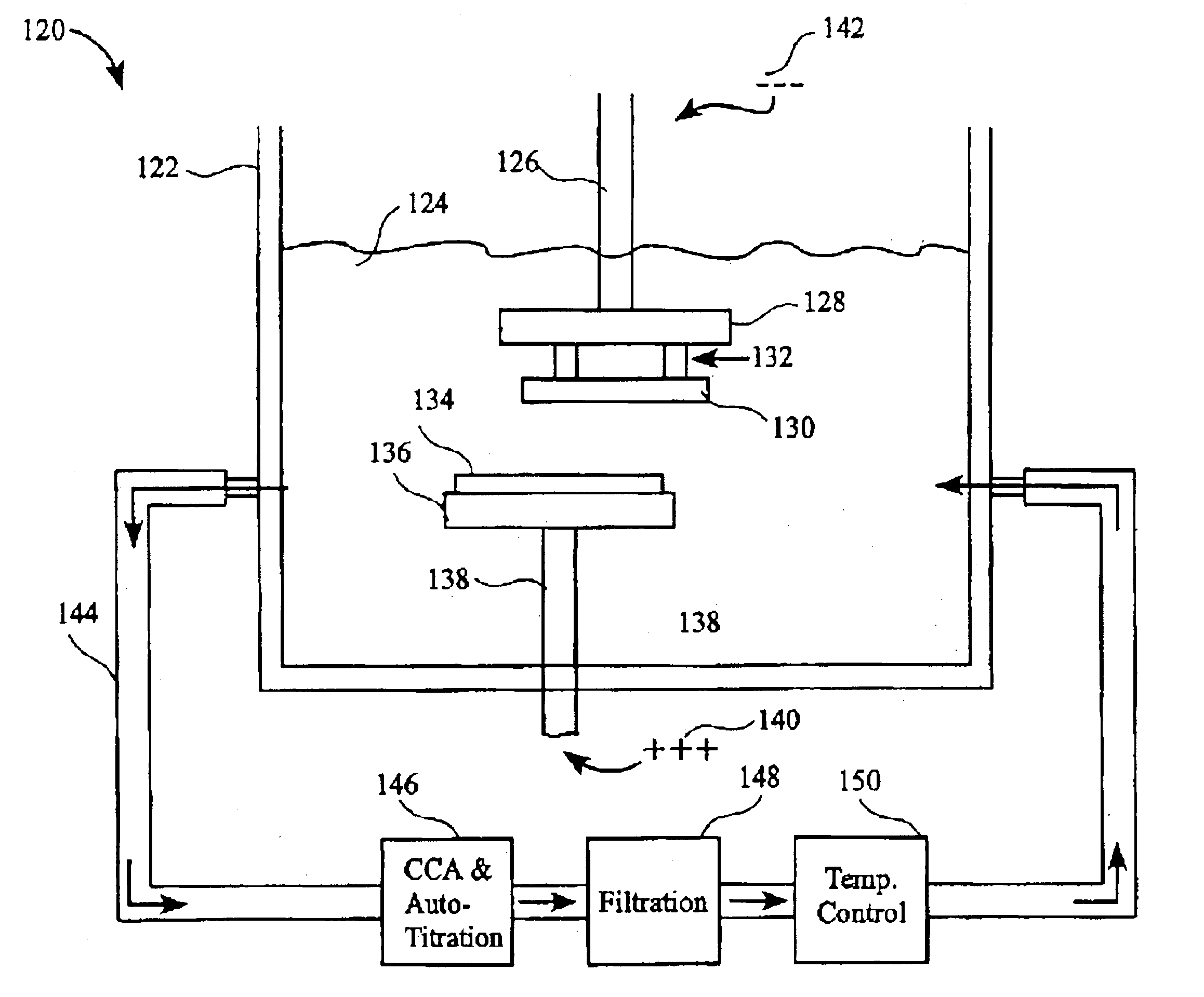
An invention for electrochemically assisted CMP for material removal and substrate planarization is disclosed. In preferred embodiments, electrochemical assisted CMP includes electrochemical formation of a weak passivation film on the surface of a substrate and material removal driven by mechanical contact with an engineered polishing substrate. In the following description, numerous specific details are set forth in order to provide a thorough understanding of the present invention. It will be understood, however, to one skilled in the art, that the present invention may be practiced without some or all of these specific details. In other instances, well known process operations have not been described in detail in order not to unnecessarily obscure the present invention.

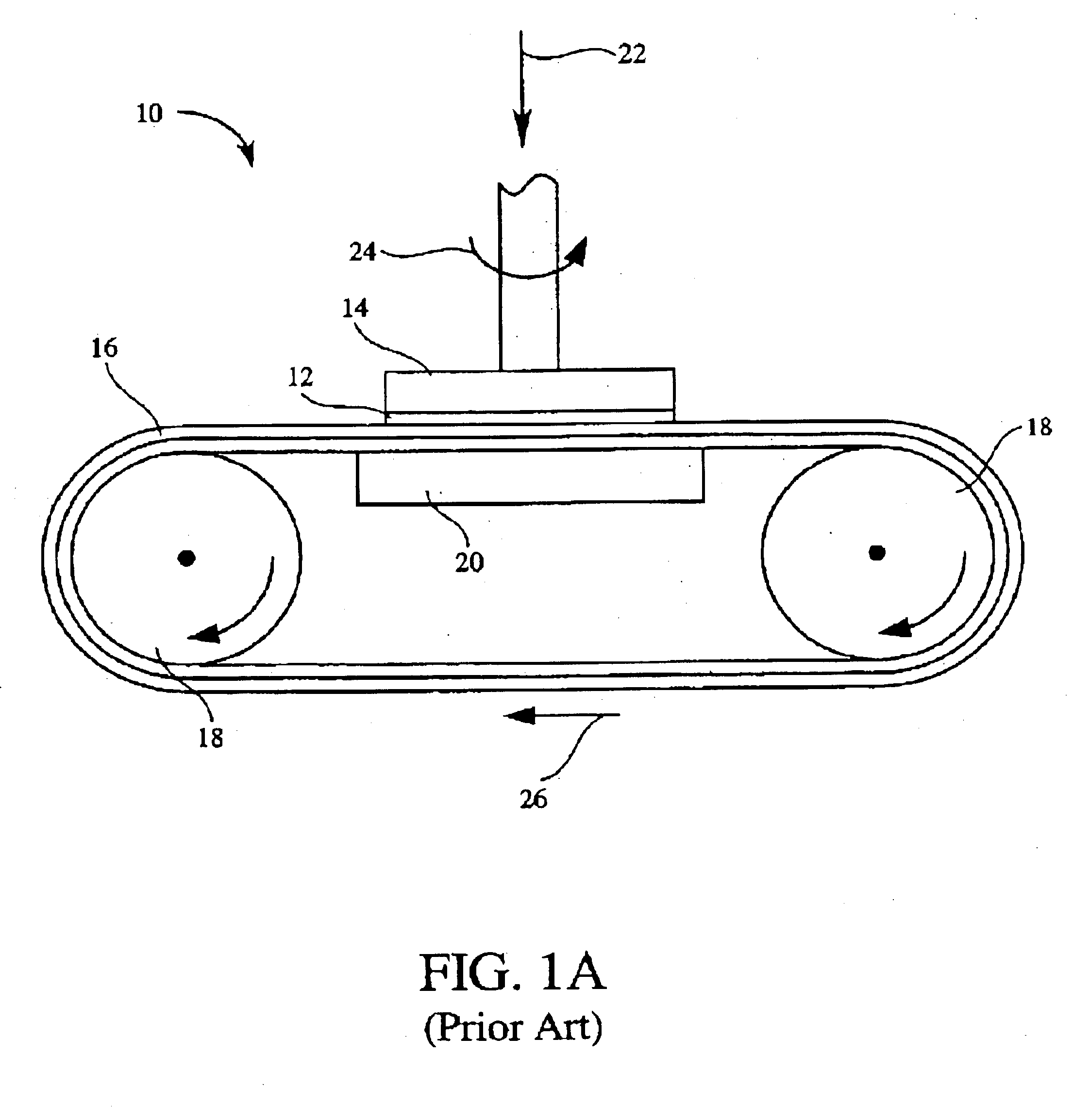
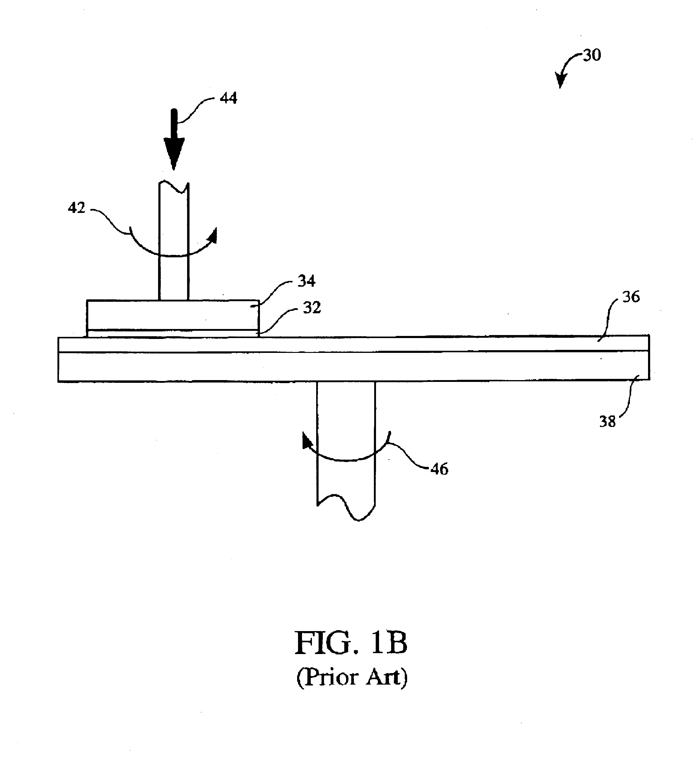
As an overview, embodiments of the present invention provide for a combination of electrochemical dissolution with low stress mechanical abrasion. A process of electropolishing uses controlled, minimal electrochemi...


PUM

PropertyMeasurementUnit
surface roughnessaaaaaaaaaa

Abstract

A method for material removal and planarization of a substrate includes formation of a weak passivating film on overburden to be removed in the presence of an electrolyte bath and an applied electric potential. An engineered polishing substrate is brought into compliance with the weak passivating film, and using low pressure to minimize shear stress realized at the surface of the substrate, material removal is controlled by mechanical contact between the polishing substrate and the weak passivating film. The weak passivating film is periodically reformed, and mechanical contact continued until desired material removal and substrate planarization is achieved.

Description

BACKGROUND OF THE INVENTION1. Field of the InventionThe present invention relates generally to the planarization of substrates, and more specifically to methods and apparatus for low stress metallization removal and substrate planarization.2. Description of the Related ArtIn the fabrication of semiconductor devices, integrated circuits are defined on semiconductor wafers by forming a plurality of layers over one another resulting in multilevel structures. Features such as trenches, vias, interconnect lines, and the like are defined within and through one or more layers, typically followed by the deposition of metallization or other conductive material fill, hereinafter referred to as conductive fill, over the defined pattern features. Chemical Mechanical Planarization (CMP) is one fabrication process used to remove overburden resulting from conductive fill deposition, and to planarize the surface of a semiconductor wafer in which a surface topography develops as a result of the vari...

Claims


Application Information

Patent Timeline
Patent Type & Authority Patents(United States)
IPC IPC(8): C25B15/00C25D17/00B23H5/08B24B37/04
CPCB24B37/20B23H5/08
Inventor KISTLER, RODNEY C.
Owner APPLIED MATERIALS INC
Why Eureka
Try Eureka