Method of forming DRAM capacitors with protected outside crown surface for more robust structures

a technology of dram capacitors and crown capacitors, applied in the direction of capacitors, semiconductor devices, electrical equipment, etc., can solve the problems of reduced available area for making capacitors, damage during subsequent processing, and difficulty in forming these fragile freestanding capacitor bottom electrodes, so as to improve the strength and increase the capacitance. , the effect of reducing processing damag

Active Publication Date: 2005-04-05
TAIWAN SEMICON MFG CO LTD
View PDF5 Cites 63 Cited by
  • Summary
  • Abstract
  • Description
  • Claims
  • Application Information

AI Technical Summary

Benefits of technology

[0013]A principal object of the present invention is to make a high-density array of crown capacitor structures having increased height for increased capacitance while reducing processing damage.

Problems solved by technology

Therefore, it is difficult to form these fragile freestanding capacitor bottom electrodes without resulting in damage during subsequent processing.
However, the available area for making the capacitor is substantially reduced since the outside surface area of the bottom electrode is not used for capacitance.
Because of the extreme height and narrow base, the bottom electrode structure is not sturdy, and is prone to damage during subsequent processing.
Unfortunately, due to non-uniform loading effects and etching variations across the wafer, non-uniform etching of the ILD layer between the closely spaced bottom electrodes 20 results in poor etch uniformity between the capacitor bottom electrodes and across the wafer, and results in unacceptably large variations in capacitance among individual memory cells when the capacitors are completed.

Method used


Image

  • Method of forming DRAM capacitors with protected outside crown surface for more robust structures
  • Method of forming DRAM capacitors with protected outside crown surface for more robust structures
  • Method of forming DRAM capacitors with protected outside crown surface for more robust structures

Examples


Embodiment Construction

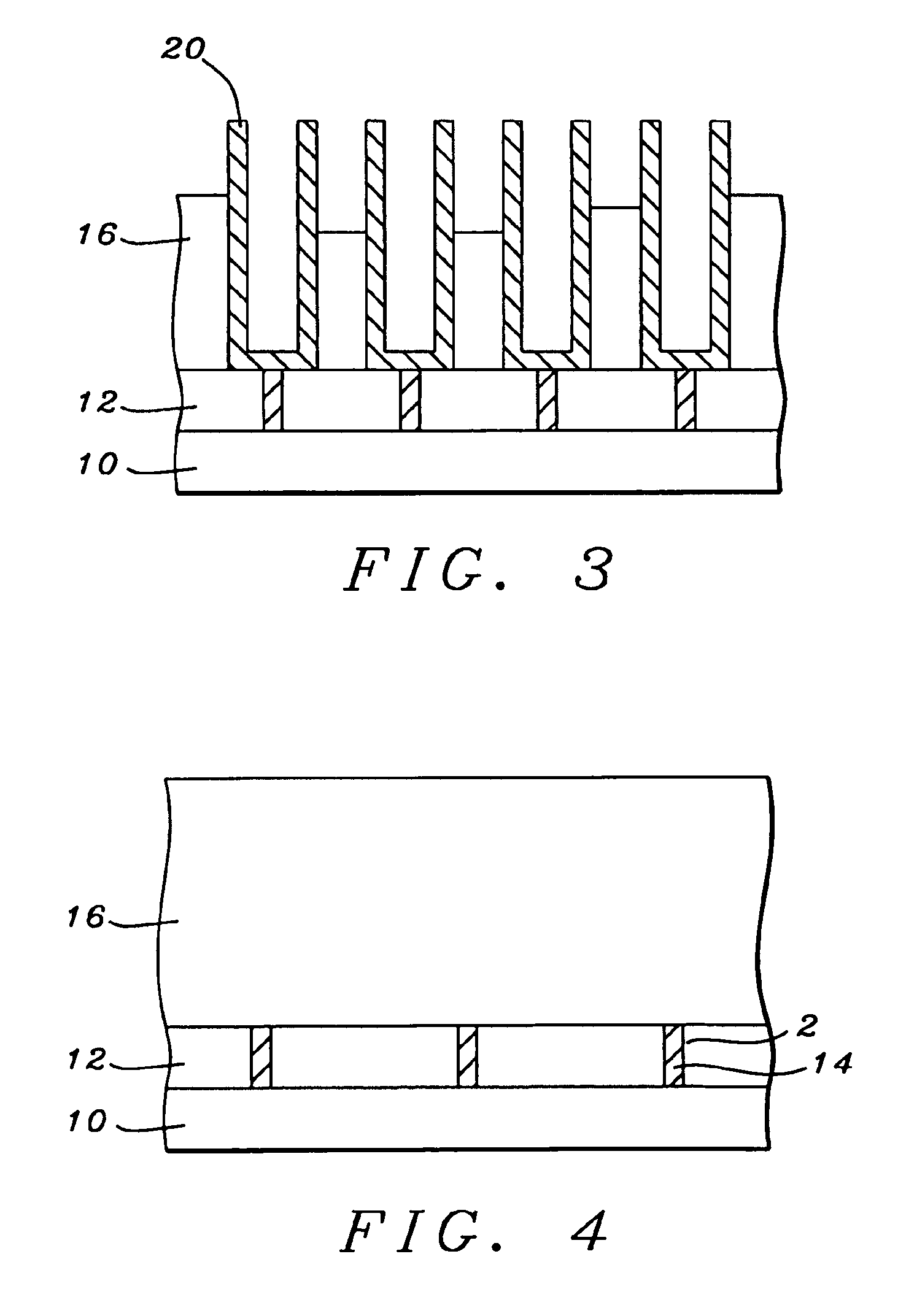
ross-sectional view of the crown capacitor structure of FIG. 10C through the portion 11-11′ and depicting the exposed outer sidewalls of the bottom electrodes for increased capacitance.

[0027]FIG. 12 is a schematic cross-sectional view of the crown capacitor structure of FIG. 10C through the portion 12-12′ and depicting the insulating support joining four adjacent capacitors.

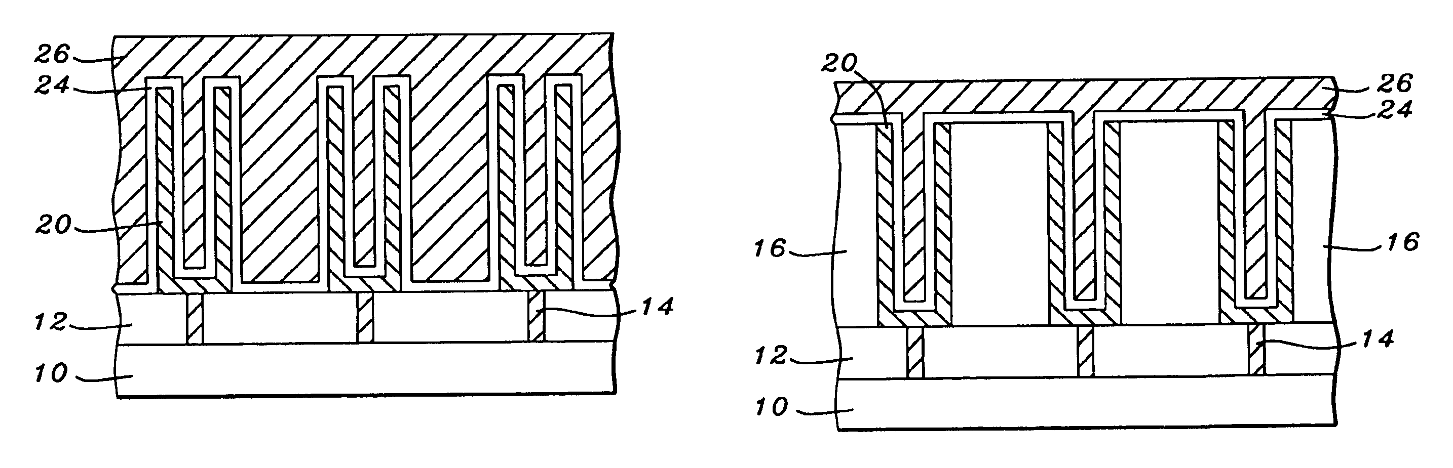
[0028]FIGS. 13 and 14 are schematic cross-sectional views showing the completed capacitors after forming the interelectrode dielectric layer and the top electrode plates.

DESCRIPTION OF THE PREFERRED EMBODIMENTS

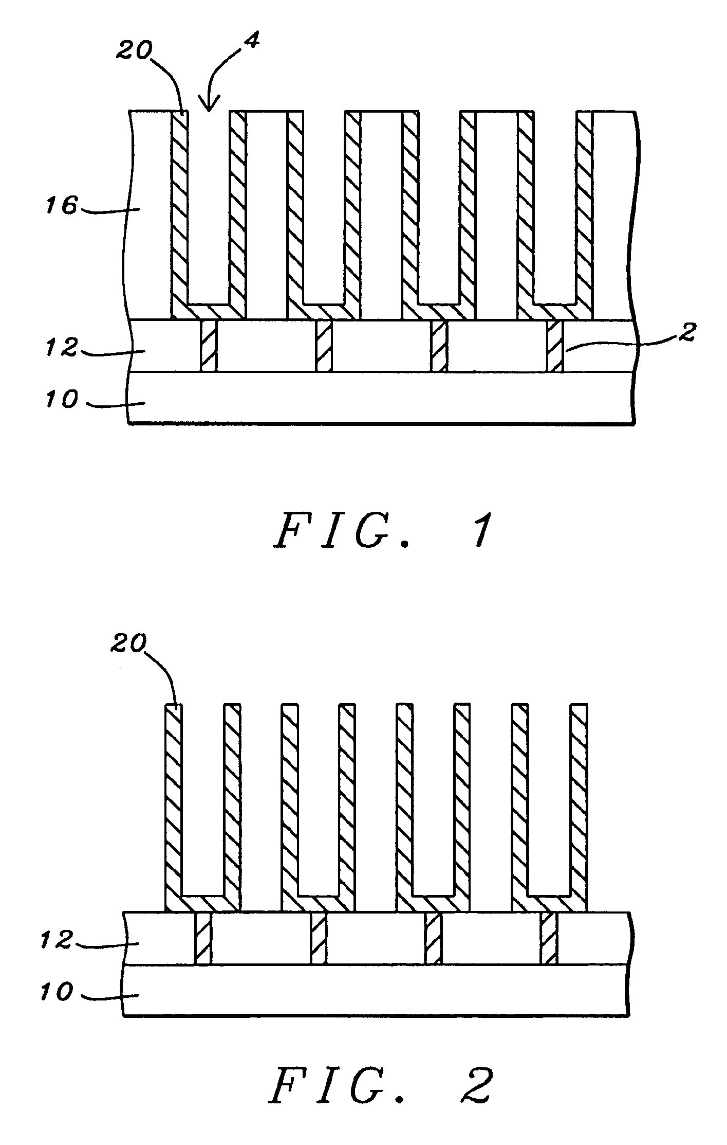
[0029]The method for making an array of improved crown capacitors is now described in detail. The invention utilizes portions of an interlevel dielectric structure between capacitors to reduce subsequent processing damage while utilizing the remaining exposed outer surface (>50%) for increasing the capacitance. Although the drawings depict a method for making capacitor bottom electrode structures having ess...


PUM


Abstract

A method for fabricating a high-density array of crown capacitors with increased capacitance while reducing process damage to the bottom electrodes is achieved. The process is particularly useful for crown capacitors for future DRAM circuits with minimum feature sizes of 0.18 micrometer or less. A conformal conducting layer is deposited over trenches in an interlevel dielectric (ILD) layer, and is polished back to form capacitor bottom electrodes. A novel photoresist mask and etching are then used to pattern the ILD layer to provide a protective interlevel dielectric structure between capacitors. The protective structures prevent damage to the bottom electrodes during subsequent processing. The etching also exposes portions of the outer surface of bottom electrodes for increased capacitance (>50%). In a first embodiment the ILD structure is formed between pairs of adjacent bottom electrodes, and in a second embodiment the ILD structure is formed between four adjacent bottom electrodes.

Description

BACKGROUND OF THE INVENTION[0002](1) Field of the Invention[0003]This invention relates to semiconductor integrated circuit devices, and more particularly relates to a method for making dynamic random access memory (DRAM) crown capacitors with improved physical strength. The process is particularly useful for crown capacitors for the next generation of DRAM circuits with minimum feature sizes of 0.18 micrometer (um) and less. The invention uses a protective interlevel dielectric (ILD) structure between capacitors while utilizing most of the outer surface (>50%) for increasing the capacitance.[0004](2) Description of the Prior Art[0005]Dynamic random access memory (DRAM) circuits (devices) are used extensively in the electronics industry, and more particularly in the computer industry for storing data in binary form (1s and 0s) as charge on a storage capacitor. These DRAM devices are made on a semiconductor substrate (or wafer), and then the substrate is diced to form the individu...

Claims


Application Information

Patent Timeline
Patent Type & Authority Patents(United States)
IPC IPC(8): H01L21/70H01L21/8242H01L27/108H01L21/02H01L21/336H01L27/02
CPCH01L28/91H01L27/10852H01L27/0207H01L27/10817H10B12/318H10B12/033
Inventor LIN, CHUN-CHIEHCHAO, LAN-LINLIN, CHIA-HUIYANG, FU-LIANGTSAI, CHIA-SHIUNGHU, CHANMING
Owner TAIWAN SEMICON MFG CO LTD
Why Eureka
Try Eureka