High adhesion triple layered anisotropic conductive adhesive film

a conductive adhesive and triple-layer technology, applied in the field of triple-layer anisotropic conductive adhesives, can solve the problems of disadvantageous degradation of flip chip packages, high cost, and complex final products, and achieve the effects of enhancing the adhesion force of a general single-layer acf, strong adhesion strength, and reducing thermal coefficien

Inactive Publication Date: 2005-04-12
KOREA ADVANCED INST OF SCI & TECH
View PDF5 Cites 56 Cited by
  • Summary
  • Abstract
  • Description
  • Claims
  • Application Information

AI Technical Summary

Benefits of technology

Accordingly, the present invention has been made to solve the above problems and it is an object of the present invention to provide a triple layered ACA film which still has strong adhe...

Problems solved by technology

However, the electronic packaging technique for packaging the above devices does not catch up with the rapid development of the semiconductor art.
However, the conventional flip chip bonding technique employs a complicated bonding process using solder including the steps of: coating solder flux on a substrate; aligning the substrate having surface electrodes with a chip having solder bumps; reflowing the solder bumps; removing remaining flux; and filling and hardening underfill.
This disadvantageously makes the process complicated and final products expensive.
However, where the substrate 50 is a glass substrate such as ...

Method used


Image

  • High adhesion triple layered anisotropic conductive adhesive film
  • High adhesion triple layered anisotropic conductive adhesive film
  • High adhesion triple layered anisotropic conductive adhesive film

Examples


Embodiment Construction

The following detailed description will present a preferred embodiment of the invention in reference to the accompanying drawings.

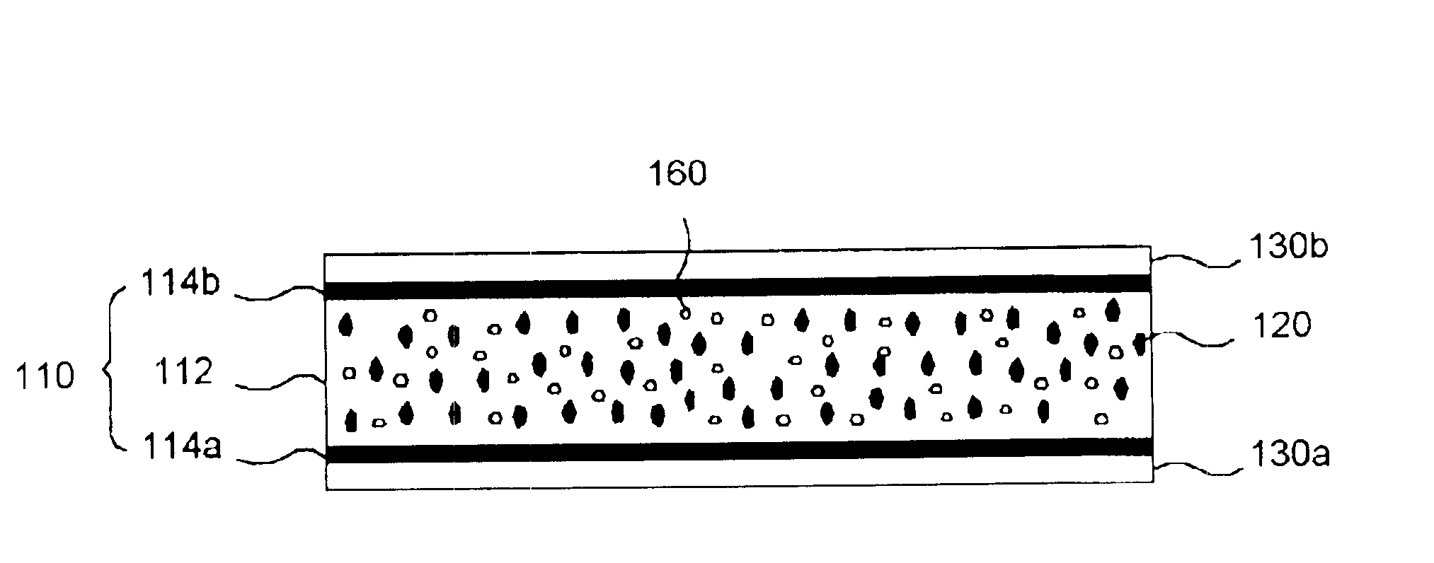
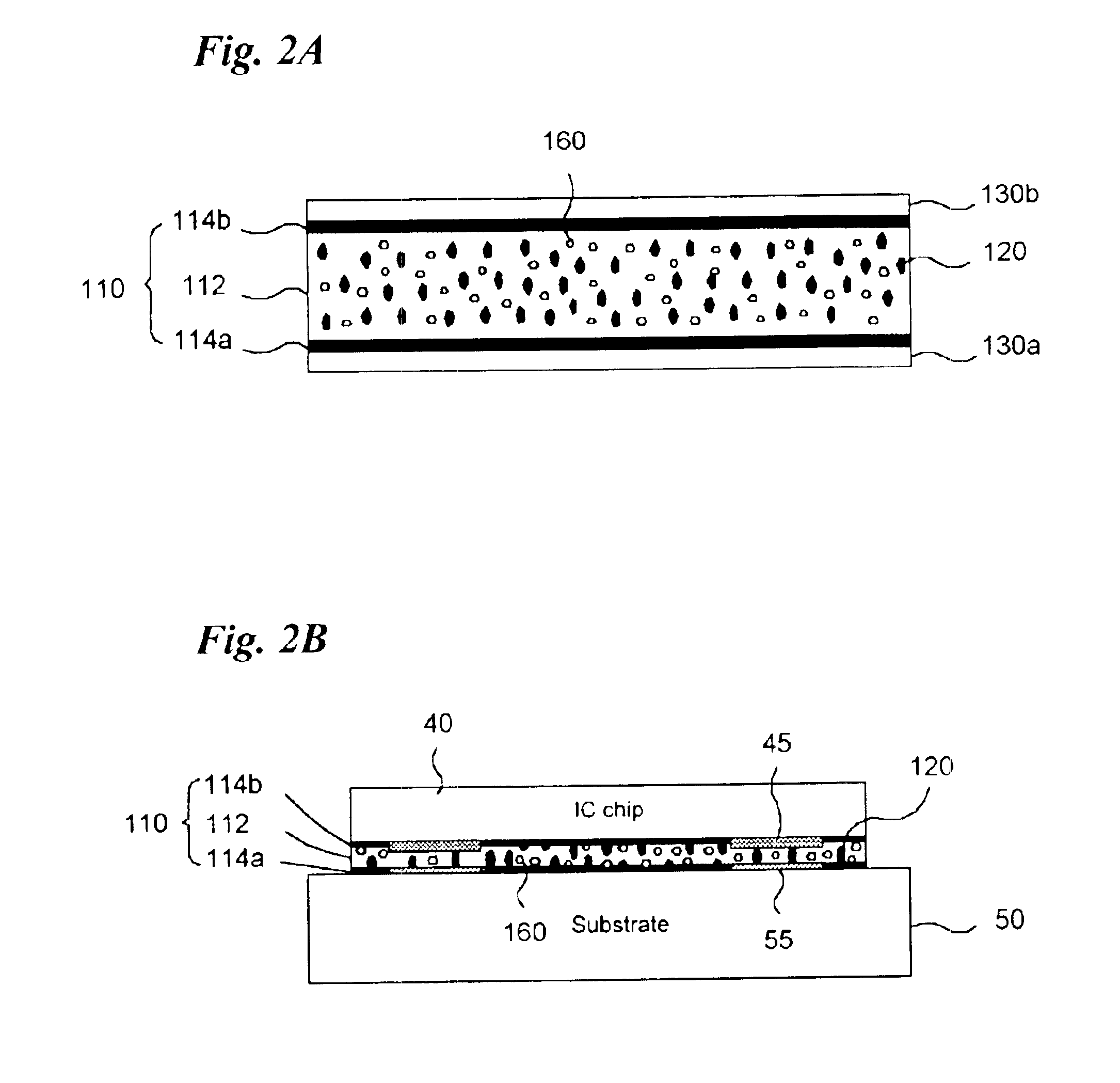
Referring to FIG. 2A, an ACA film 110 of the invention has a tripe layered structure defined by a lower adhesion reinforcing layer 114A, a main ACA film 112 and an upper reinforcing layer 114B.

The main ACA film 112 is made of an epoxy resin-based material, and has a structure in which conductive particles 120 having a size range of about 3 to 10 μm and non-conductive particles 160 having a size range of 0.1 to 1 μm, are finely dispersed.

The main ACA film 112 is interposed between the lower adhesion reinforcing layer 114a and the upper adhesion reinforcing layer 114b. The lower and upper adhesion reinforcing layers 114a and 114b each is made of epoxy resin-based material and have a thickness range of 1 to 10 μm. The lower and upper adhesion reinforcing layers 114a and 114b each may further contain the conductive particles by 5 to 10% by weight in order to ...


PUM

PropertyMeasurementUnit
Lengthaaaaaaaaaa
Lengthaaaaaaaaaa
Percent by massaaaaaaaaaa

Abstract

Disclosed is a triple layered ACA film adapted for enhancing the adhesion strength of a typical single layer Anisotropic Conductive Film or for enhancing the adhesion strength of the ACA film in flip chip bonding. The triple layered ACA film of the invention comprises: a main ACA film based upon epoxy resin and containing conductive particles having a particle size of 3 to 10 μm and optionally non-conductive particles having a particle size of 0.1 to 1 μm; and adhesion reinforcing layers based upon epoxy resin and formed at both sides of the main ACA film.

Description

BACKGROUND OF THE INVENTION1. Field of the InventionThe present invention relates to an anisotropic conductive adhesive (ACA) film, and more particularly, a triple layered ACA film adapted for enhancing the adhesion strength of a typical single layer anisotropic Conductive Film (ACF) or for enhancing the adhesion strength of the ACA film in flip chip bonding.2. Description of the Related ArtAs well known in the art, the electronic packaging is a wide-ranging and various system fabricating technique including all processes related to from semiconductor device to final product. According to the sharply developing recent semiconductor technology, more than millions of cells are integrated while non-memory devices are developing with a tendency toward many I / O pin numbers, large die size, heat emission by a large quantity, high electric performance and so on. However, the electronic packaging technique for packaging the above devices does not catch up with the rapid development of the s...

Claims


Application Information

Patent Timeline
IPC IPC(8): B32B27/38H01L21/60H01L21/02H05K3/32C09J7/02C09J7/00C09J9/02C09J163/00C09J171/10H01B5/16H01R11/01
CPCB32B27/38H01L24/83H05K3/323H01L24/29Y10T428/26H01L2224/29499H01L2224/32225H01L2224/83101H01L2224/8319H01L2224/838H01L2924/01004H01L2924/01005H01L2924/01047H01L2924/01079H01L2924/01082H01L2924/0781H01L2924/14H05K2201/10674H05K2203/1189H01L2224/2919H01L2924/01006H01L2924/01033H01L2924/01068H01L2924/01087H01L2924/014H01L2924/0665H01L2224/29101Y10T428/263Y10T428/25Y10T428/28Y10T428/24967Y10T428/265Y10T428/24975Y10T428/2848Y10T428/287Y10T428/266H01L2224/83851H01L2924/07811H01L2924/10253H01L2924/00H01L2924/351Y10T428/31511Y10T428/31515B32B27/08
Inventor PAIK, KYUNG WOOKYIM, MYUNG JIN
Owner KOREA ADVANCED INST OF SCI & TECH
Why Eureka
Try Eureka