Alloying method for a image display device using laser irradiation

a technology of laser irradiation and image display, which is applied in the direction of identification means, semiconductor devices, instruments, etc., can solve the problems of thermal alloying process degradation of device characteristics, increase production costs, and reduce throughput, and achieve excellent performance

Inactive Publication Date: 2005-04-12
SONY CORP
View PDF24 Cites 8 Cited by
  • Summary
  • Abstract
  • Description
  • Claims
  • Application Information

AI Technical Summary

Benefits of technology

With this configuration, since a desirable ohmic contact can be formed between a device and an electrode...

Problems solved by technology

In this case, if the n-GaAs layer is directly formed on a GaAs substrate, there is no problem; however, if an epitaxial layer not withstanding the above heating temperature is formed under the n-GaAs layer, or if an insulating film made from a resin or the like is formed before formation of a contact metal, there may occur a problem that device characteristics may be degraded by the thermal alloying proce...

Method used


Image

  • Alloying method for a image display device using laser irradiation
  • Alloying method for a image display device using laser irradiation
  • Alloying method for a image display device using laser irradiation

Examples


Embodiment Construction

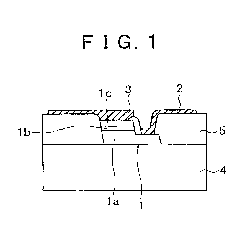
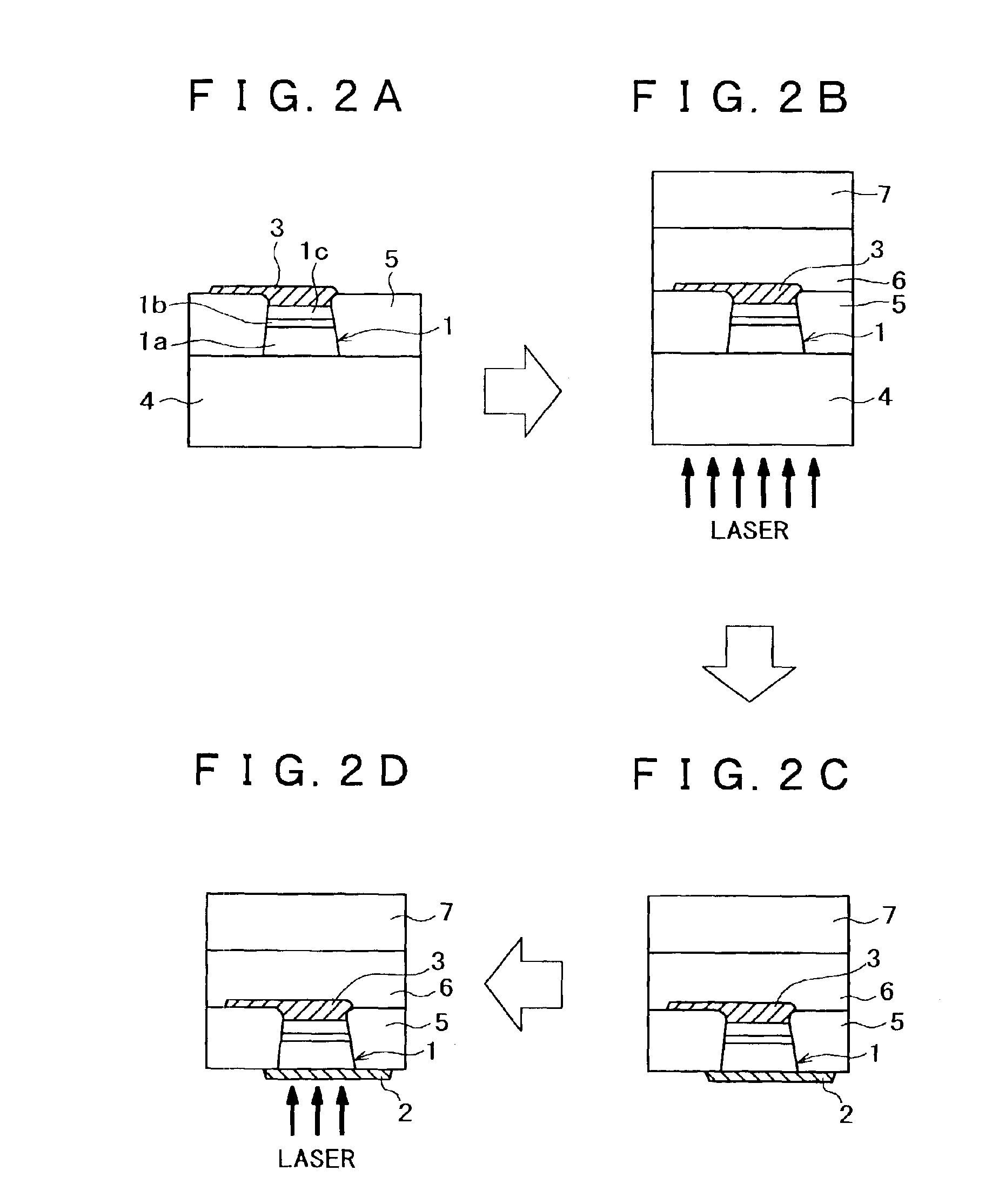
Hereinafter, an alloying method, a wiring forming method, a display device forming method, and an image display unit fabricating method according to the present invention will be described with reference to the drawings.

Embodiments of the alloying method and the wiring forming method according to the present invention will be first described. In these embodiments, an electrode is alloyed with a micro LED representative of a semiconductor device by using the alloying method of the present invention.

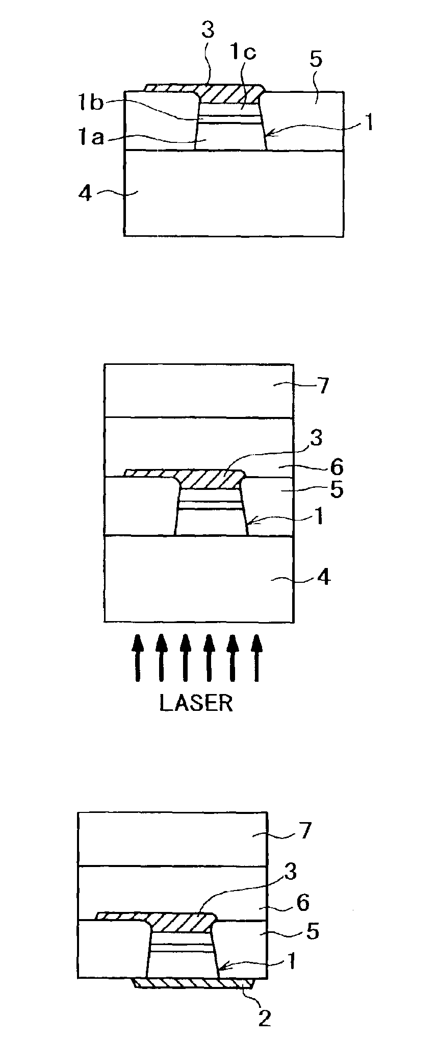
As shown in FIG. 1, a micro LED 1 is composed of an n-cladding layer 1a, an active layer 1b, and a p-cladding layer 1c, wherein an n-electrode 2 is connected to the n-cladding layer 1a and a p-electrode 3 is connected to the p-cladding layer 1c.

In general, the n-electrode 2 and the p-electrode 3 are formed, as shown in FIG. 1, by forming an insulating layer 5 so as to cover the micro LED 1 on a GaAs substrate 4, and providing openings in portions, corresponding to the n-cladding layer 1a ...


PUM


Abstract

An alloying method includes steps of forming a metal layer on a semiconductor that is then transferred to a material having a low thermal conductivity. An interface between the semiconductor and the metal layer is formed into an alloy by irradiating the interface with a laser beam having a wavelength that is absorbable in at least one of the semiconductor and the metal layer. Preferably, the material having a low thermal conductivity is a resin or amorphous silicon. Because the entire semiconductor is not heated and only a necessary portion is locally heated, the necessary portion can be readily alloyed to be converted into an ohmic contact without exerting adverse effects on the characteristics of the semiconductor device.

Description

This application claims priority to Japanese Patent Application Number JP2002-009154 filed Jan. 17, 2002 and Japanese Patent Application Number JP2002-362214 filed Dec. 13, 2002, both of which are incorporated herein by reference.BACKGROUND OF THE INVENTIONThe present invention relates to a method of alloying an interface between a semiconductor and a metal layer, thereby forming an ohmic contact, and to a wiring forming method, a display unit forming method, and an image display unit fabricating method using the alloying method.In the case of forming a metal layer as an electrode on a semiconductor device, it is required to convert a portion, being in contact with the semiconductor device, of the electrode into an ohmic contact to the semiconductor device. The conversion of a portion of an electrode into an ohmic contact has been typically performed by thermally alloying the portion of the electrode with the semiconductor device. For example, in the case of converting a portion, be...

Claims


Application Information

Patent Timeline
IPC IPC(8): H01L21/70H01L21/02H01L21/268H01L21/768H01L33/00G09F9/00H01L21/28G09F9/30G09F9/33H01L21/60H01L33/32H01L33/40H01L33/56
CPCH01L21/268H01L21/76886H01L24/24H01L24/82H01L33/0095H01L2924/12041H01L2924/01033H01L2924/01006H01L2924/01005H01L2924/10329H01L2221/68359H01L2221/68368H01L2224/24137H01L2224/24225H01L2224/24226H01L2224/32225H01L2224/73267H01L2924/01002H01L2924/01004H01L2924/01012H01L2924/01013H01L2924/01015H01L2924/01039H01L2924/01046H01L2924/01078H01L2924/01079H01L2924/00H01L2924/12042
Inventor TOMODA, KATSUHIROOHATA, TOYOHARU
Owner SONY CORP
Why Eureka
Try Eureka