
Ceramic substrate and process for producing the same

a technology of ceramic substrate and substrate, which is applied in the direction of manufacturing tools, hot plate heating arrangements, and testing/measurement of semiconductor/solid-state devices, etc., can solve the problems of leakage current between the electrodes or between the resistance heating elements at high temperature, cracks start to be generated, and the like, so as to prevent the element from disconnection and the like, high ohmic resistance value, and high thickness

Inactive Publication Date: 2005-04-12
IBIDEN CO LTD
View PDF27 Cites 12 Cited by
  • Summary
  • Abstract
  • Description
  • Claims
  • Application Information

AI Technical Summary

Benefits of technology

The present invention is a ceramic substrate with a conductor layer that has a peaked shape at its edge. This design solves problems that arise when the substrate is exposed to thermal shock or high temperatures. The substrate can function as a hot plate or an electrostatic chuck depending on the conductor layer's design. The conductor layer is printed on a ceramic green sheet and then integrated with another green sheet before being sintered. The technical effect of this invention is to improve the performance and reliability of ceramic substrates in high-temperature applications.

Problems solved by technology

However, in ceramic substrates produced by such a process, problems as follows arise: cracks start to be generated at edges of their conductor layer such as a resistance heating element when thermal shock is given to the substrates; or a high temperature area is generated along the resistance heating element.
Furthermore, a scatter is generated in chuck power so that sufficient adsorption power cannot be obtained.
About an internal electrode or a resistance heating element, a leakage current between the electrodes or between the resistance heating elements at high temperature comes into a problem.

Method used


Image

  • Ceramic substrate and process for producing the same
  • Ceramic substrate and process for producing the same
  • Ceramic substrate and process for producing the same

Examples


example 1

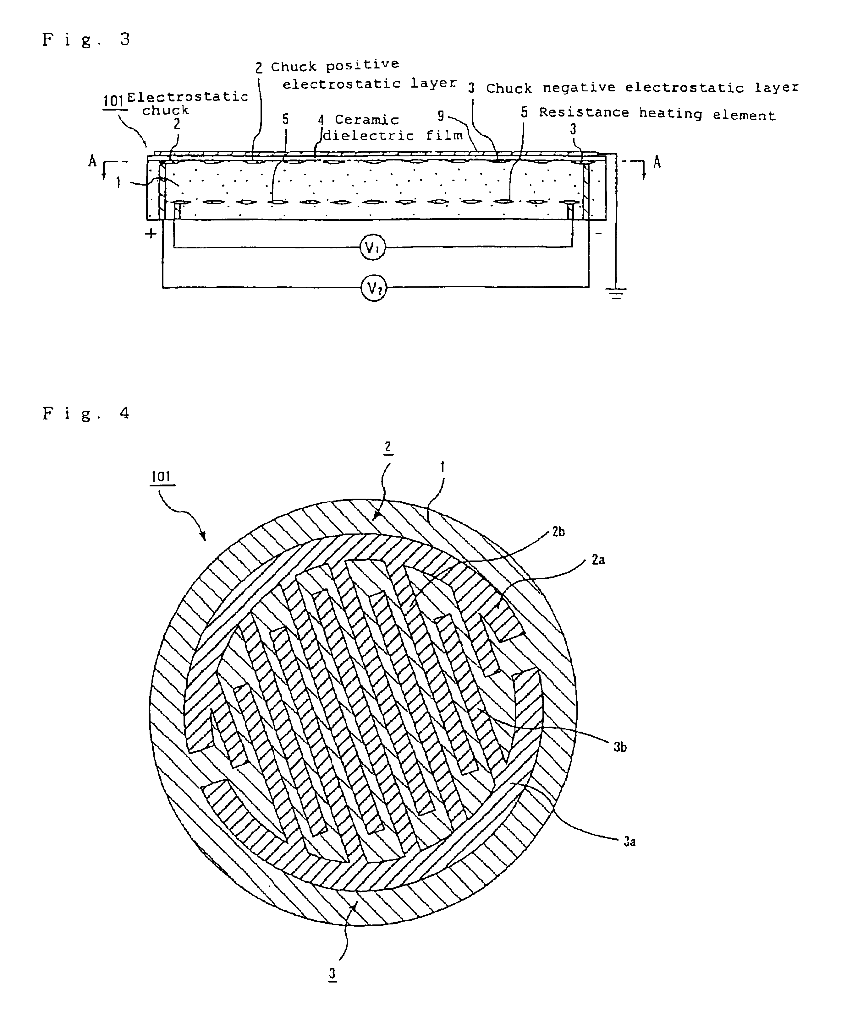
Production of an Electrostatic Chuck (See FIG. 3)

(1) The following paste was used to conduct formation by doctor blade method to obtain a green sheet 0.47 μm in thickness: a paste obtained by mixing 100 parts by weight of aluminum nitride powder (made by Tokuyama Corp., average particle diameter: 1.1 μm) 4 parts by weight of yttria (average particle diameter: 0.4 μm), 11.5 parts by weight of an acrylic binder, 0.5 part by weight of a dispersant and 53 parts by weight of mixed alcohols of 1-butanol and ethanol.(2) Next, this green sheet was dried at 80° C. for 5 hours, and subsequently the following holes were made by punching: holes which would be through holes through which semiconductor wafer supporting pins 1.8 mm, 3.0 mm and 5.0 mm in diameter were inserted; and holes which would be plated through holes for connecting external terminals.(3) The following were mixed to prepare a conductor containing paste A: 100 parts by weight of tungsten carbide particles having an average part...

example 2

(EXAMPLE 2)

Production of a Wafer Prober 201 (See FIG. 12)

(1) The following paste was used to conduct formation by doctor blade method to obtain a green sheet 0.47 μm in thickness: a paste obtained by mixing 1000 parts by weight of aluminum nitride powder (made by Tokuyama Corp., average particle diameter: 1.1 μm), 40 parts by weight of yttria (average particle diameter: 0.4 μm), and 530 parts by weight of mixed alcohol's of 1-butanol and ethanol.(2) Next, this green sheet was dried at 80° C. for 5 hours, and subsequently through holes for plated through holes for connecting external terminals to resistance heating elements were made by punching.(3) The following were mixed to prepare a conductor containing paste A: 100 parts by weight of tungsten carbide particles having an average particle diameter of 1 μm, 3.0 parts by weight of an acrylic binder, 3.5 parts by weight of α-terpineol solvent, and 0.3 part by weight of a dispersant.

The following were mixed to prepare a conductor cont...

example 3

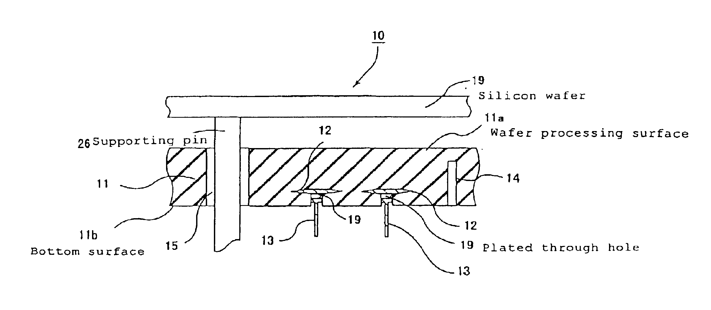
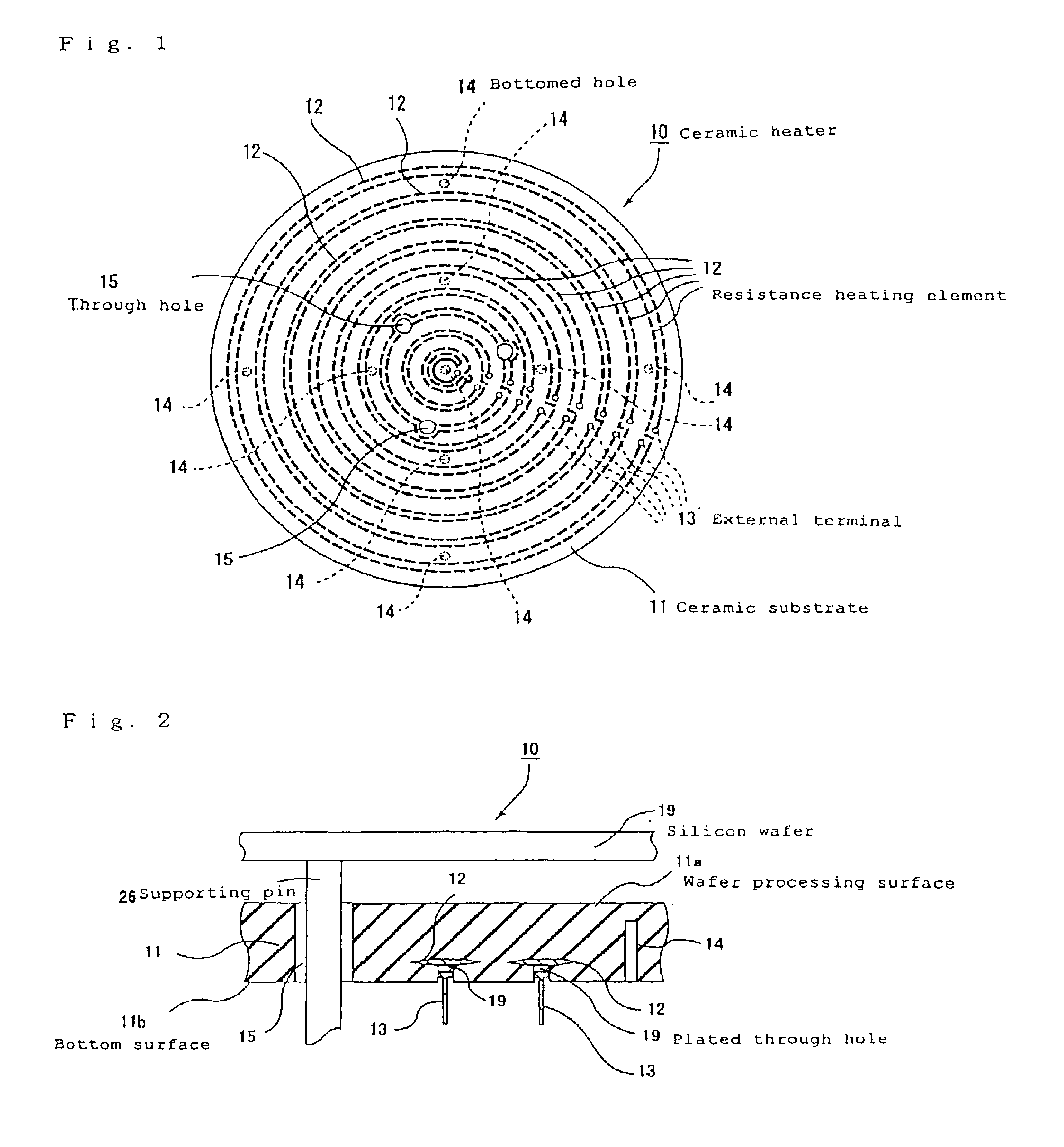
Alumina Hot Plate (See FIGS. 1 and 2)

(1) The following paste was used to conduct formation by doctor blade method to obtain green sheets 0.47 μm in thickness: a paste obtained by mixing alumina: 93 parts by weight, SiO2: 5 parts by weight, CaO: 0.5 part by weight, MgO: 0.5 part by weight, TiO2: 0.5 part by weight, an acrylic binder: 11.5 parts by weight, 0.5 part by weight of a dispersant and 53 parts by weight of mixed alcohols of 1-butanol and ethanol.(2) Next, these green sheets were dried at 80° C. for 5 hours, and subsequently the following holes were made in the green sheets for which they are necessary by punching: holes which would be through holes through which semiconductor wafer supporting pins having diameter of 1.8 mm, 3.0 mm and 5.0 mm were inserted; and holes which would be plated through holes for connecting external terminals.(3) The following were mixed to prepare a conductor containing paste B: 100 parts by weight of tungsten particles having an average particle d...


PUM

PropertyMeasurementUnit
thicknessaaaaaaaaaa
widthaaaaaaaaaa
widthaaaaaaaaaa

Abstract

It is a an object of the present invention to provide a ceramic substrate for a semiconductor producing / examining device which has high fracture toughness value, exellent thermal shock resistivity, high thermal conductivity and an excellent temperature rising and falling properties, and is preferable as a hot plate, an electrostatic chuck, a wafer prober and the like. A ceramic substrate, for a semiconductor producing / examining device, having a conductor formed inside thereof or on the surface thereof of the present invention is the ceramic substrate, wherein said ceramic substrate has been sintered such that a fractured section thereof exhibits intergranular fracture.

Description

TECHNICAL FIELDThe present invention relates to a ceramic substrate used mainly in the semiconductor industry, and particularly to a ceramic substrate that is suitable for a hot plate, an electrostatic chuck, a wafer prober and the like, and is superior in thermal shock resistance, heat uniformity, chuck power and so on.BACKGROUND ARTSemiconductors are very important goods necessary in various industries. A semiconductor chip is produced, for example, by slicing a silicon monocrystal into a predetermined thickness to produce a silicon wafer, and then forming a plurality of integrated circuits and the like on this silicon wafer.In the process for producing this semiconductor chip, a silicon wafer put on an electrostatic chuck is subjected to various treatments such as etching and CVD to form a conductor circuit, an element and the like. At this time, corrosive gas such as gas for deposition or gas for etching is used; therefore, it is necessary to protect an electrostatic electrode l...

Claims


Application Information

Patent Timeline
Patent Type & Authority Patents(United States)
IPC IPC(8): H01L21/00H01L21/683H01L21/67H05B3/22H05B3/68H05B3/74H05B3/14H05B3/26B23Q3/15H01L21/66H05B3/12H05B3/18H05B3/20
CPCH01L21/67103H01L21/6831H05B3/74H05B3/143H05B3/265H01L21/6833H05B3/18
Inventor HIRAMATSU, YASUJIITO, YASUTAKA
Owner IBIDEN CO LTD
Learn More