

Method and device for minimizing multi-layer microscopic and macroscopic alignment errors
- Summary
- Abstract
- Description
- Claims
- Application Information
AI Technical Summary
Benefits of technology
Problems solved by technology
Method used
Image

Examples
first embodiment
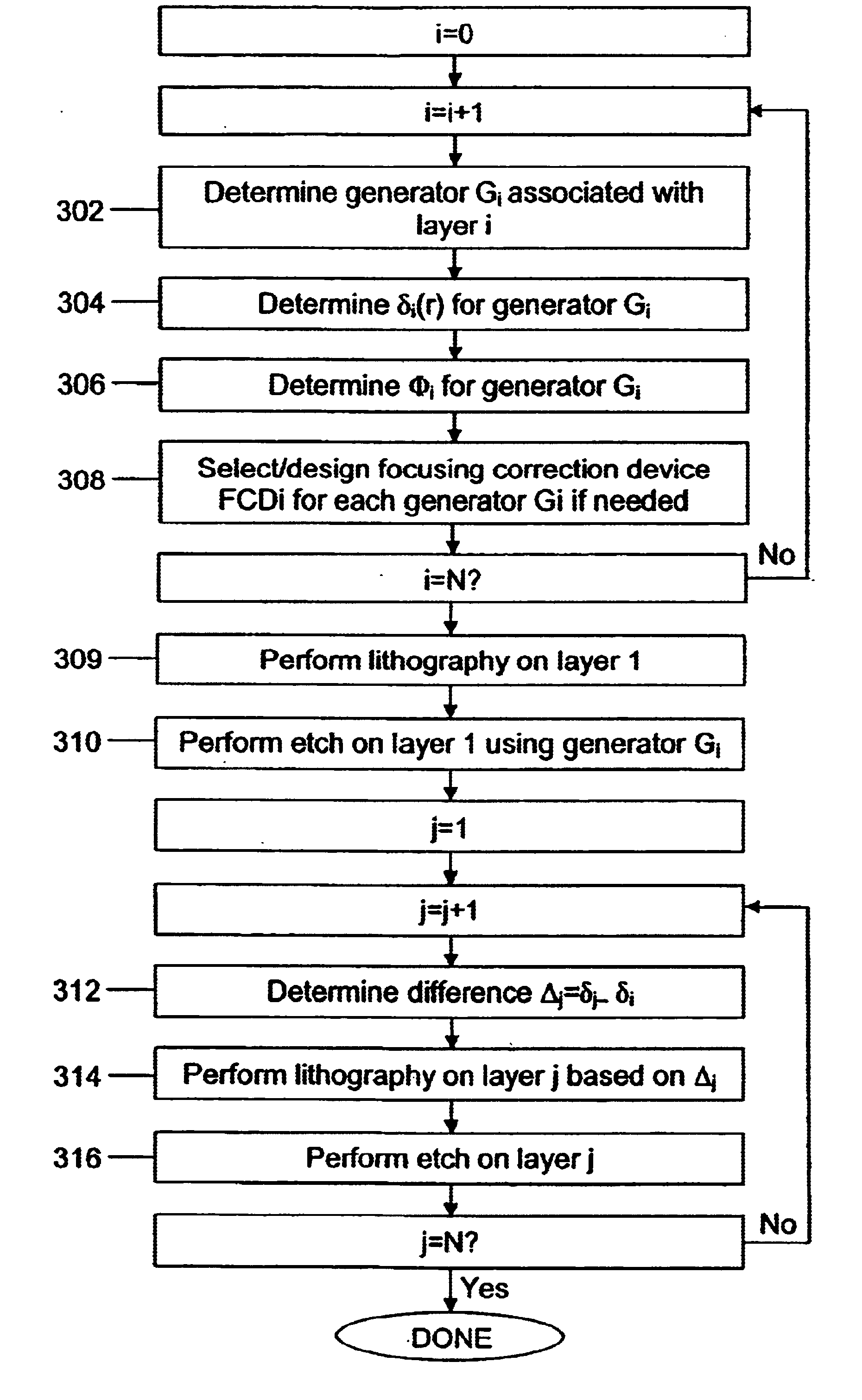
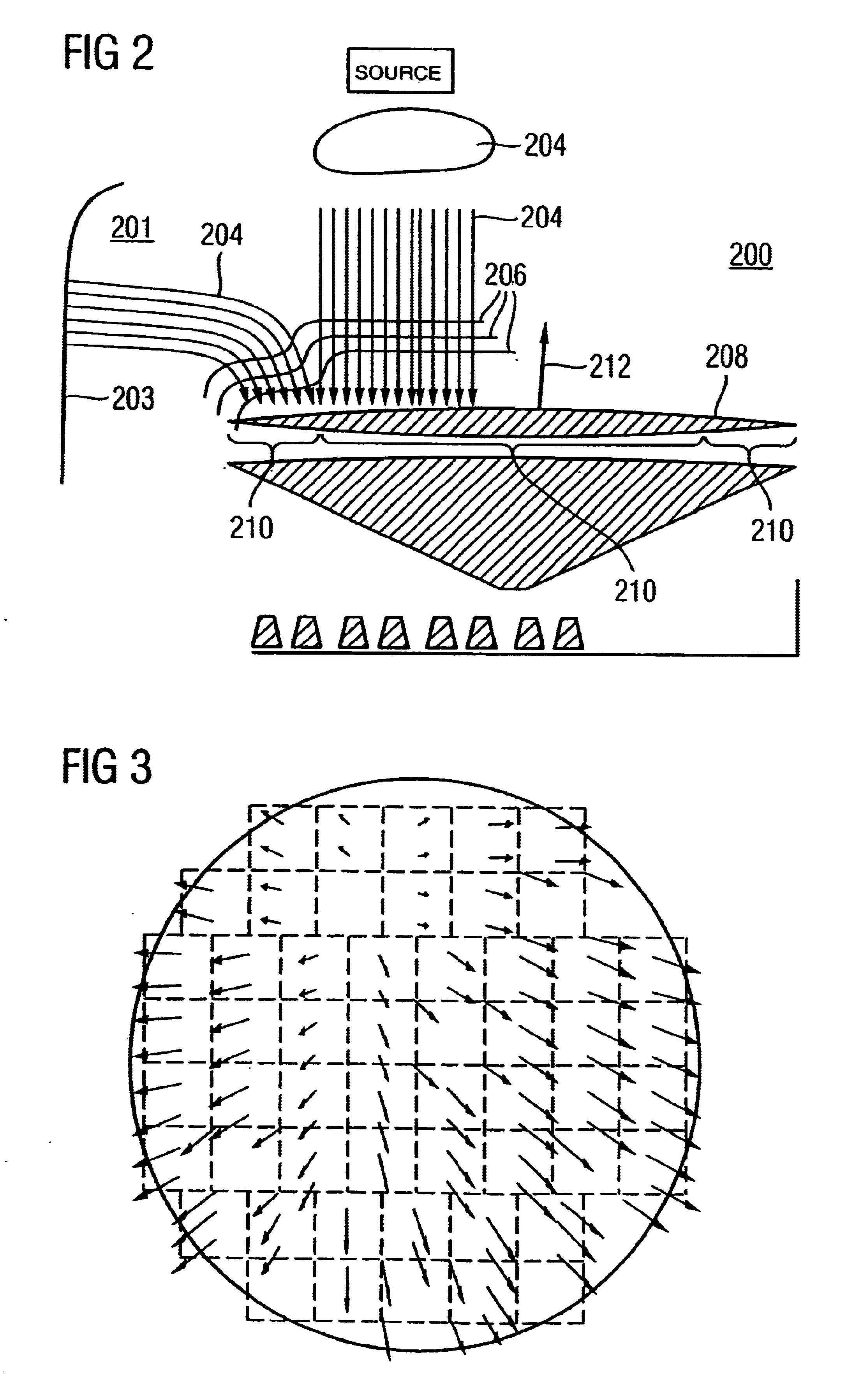
[0063]Examples of various focusing correction devices determined in step 308 to be used with a plasma etch chamber, such as the device known by the trade name of Super-e made by Applied Materials, are discussed below with respect to FIGS. 13-26. In particular, a possible focusing correction device is shown in FIGS. 13-16. The focusing correction device 400 includes a focusing collar made of an annular-like focus ring made of single crystal p-type silicon 402, having a resistivity of 0.02Ω-cm, that is placed next to the electrostatic chuck 210 and below and adjacent the wafer 208. A quartz piece 404 is placed adjacent to and below the silicon piece 402. A separate silicon piece 405 is placed directly on top of the quartz piece 404. The silicon piece 405 has a trapezoidal shape having a height H that can have a range of values and an angle α that can have a range of values as well that are determined so as to correct the shapes of the electrical isopotential surfaces and electric fiel...
second embodiment
[0066]a possible focusing correction device is shown in FIG. 17. The focusing correction device 500 includes a power coupled annular-like piece of silicon 502. In addition, a silicon piece 504 is supported above the top surface of the silicon piece 502, via one or more quartz supports 506, by an amount that ranges from approximately 0.1 mm to 5 mm. In addition, the silicon piece 504 is insulated from silicon piece 502. The silicon piece 504 has a side cross-sectional shape of a trapezoid with a height H that can have a range of values and an angle α that can have a range of values as well that are determined so as to correct the shapes of the electrical isopotential surfaces and electric fields to be the same as that of the adjacent layer. An annular gap 508 is formed between the silicon piece 504 and the wafer 208. The silicon piece 502 has a good coupling with the wafer and the electrostatic chuck while the silicon piece 504 has a poor coupling.
third embodiment
[0067]a possible focusing correction device is schematically shown in FIGS. 18-25. The focusing correction device 600 includes a focusing collar made of an annular-like focus ring made of single crystal p-type silicon 602, having a low resistivity ranging from 0.01Ω-cm to 0.05Ω-cm, that is placed next to the electrostatic chuck 603 and below and adjacent the wafer 208.
[0068]As shown in FIG. 18, the perimeter of the cylindrical-like ceramic electrostatic chuck 603 has a two-step profile. The first step has a depth d1 and a width w1. The second lower step has a shallower depth d2 and a width w2 of approximately 0.545 inches. A dielectric layer 616 made of a ceramic material that covers the top of the electrostatic chuck 603 and the first step. The dielectric layer 616 functions in a manner well known in the art. The wafer 208 is placed on top of the layer 616 as shown in FIG. 18.
[0069]A quartz material 650 is spaced from the electrostatic chuck 603 and acts as an insulator between the...
PUM
 Abstract
Description
Claims
Application Information