Monolithic three dimensional array of charge storage devices containing a planarized surface

a charge storage device and three-dimensional array technology, applied in the field of three-dimensional tft arrays, can solve the problems of single silicon plane, less than the optimal cell density, and limit the amount of data that can be stored to the number of devices

Inactive Publication Date: 2005-04-19
WODEN TECH INC
View PDF196 Cites 502 Cited by
  • Summary
  • Abstract
  • Description
  • Claims
  • Application Information

AI Technical Summary

Benefits of technology

[0036]Another preferred embodiment of the present invention provides a two- or three-dimensional memory array constructed of thin film transistors disposed above the substrate. Spaced-apart conductors disposed in a first direction form contacts with memory cells formed in rail stacks disposed in a second direction different from the first direction. A local charge trapping medium receives and stores hot electrons injected by thin film transistors formed at the intersections of the spaced-apart conductors and the rail stacks. The local charge trapping medium may be used to store charge adjacent to a transistor drain and by reversing the drain and source lines, two bits per memory cell may be stored, if desired. A programming method insures that stored memory will not be inadvertently disturbed.
[0037]Another preferred embodiment of the present invention provides a non-volatile thin film transistor (TFT) memory device that is constructed above a substrate. It employs a source, drain and channel formed of transition metal crystallized silicon. A local charge storage film is disposed vertically adjacent to the channel and stores injected charge. A two- or three-dimensional array of such devices may be constructed above the substrate. Spaced-apart conductors disposed in a first direction form contacts with memory cells formed in rail stacks disposed in a second direction different from the first direction. The local charge storage film receives and stores charge injected by TFTs formed at the intersections of the spaced-apart conductors and the rail stacks. The local charge storage film may be used to store charge adjacent to a transistor drain and by reversing the drain and source lines, two bits per memory cell may be stored, if desired. A programming method insures that stored memory will not be inadvertently disturbed.

Problems solved by technology

Unfortunately, these devices are typically fabricated in a single crystalline silicon substrate and therefore are limited to two-dimensional arrays of storage devices, thereby limiting the amount of data that can be stored to the number of devices that can be fabricated in a single plane of silicon.
This cell area is larger than desirable, and leads to a less than optimum cell density.
The holes cannot flow well through the oxide and consequently build up near the surface.
Therefore, each cell in this layout is not fully self-aligned, because the contact pads and the contact vias are each patterned using a non-self aligned photolithography step.
Therefore, each memory cell has an area that is larger than desirable, and leads to a less than optimum cell density.
The memory cell of Koyama is also complex to fabricate because it requires the formation of contact pads and bit line contact vias.
Furthermore, the manufacturability of the device of Koyama is less than optimum because both bit lines and word lines have a non-planar top surface due to the non-planar underlying topography.
This may lead to open circuits in the bit and word lines.
The above described prior art devices are relatively expensive because their density is not optimized.

Method used


Image

  • Monolithic three dimensional array of charge storage devices containing a planarized surface
  • Monolithic three dimensional array of charge storage devices containing a planarized surface
  • Monolithic three dimensional array of charge storage devices containing a planarized surface

Examples


second embodiment

[0123]As will be discussed below, the charge trapping memory device of the present embodiment can be fabricated with one of two general structures. In one embodiment the charge storage medium is formed adjacent to the semiconductor region and in a second embodiment the charge storage medium is formed above or below the semiconductor region.

1. A Three Terminal Pillar Memory with Adjacent Charge Storage Medium

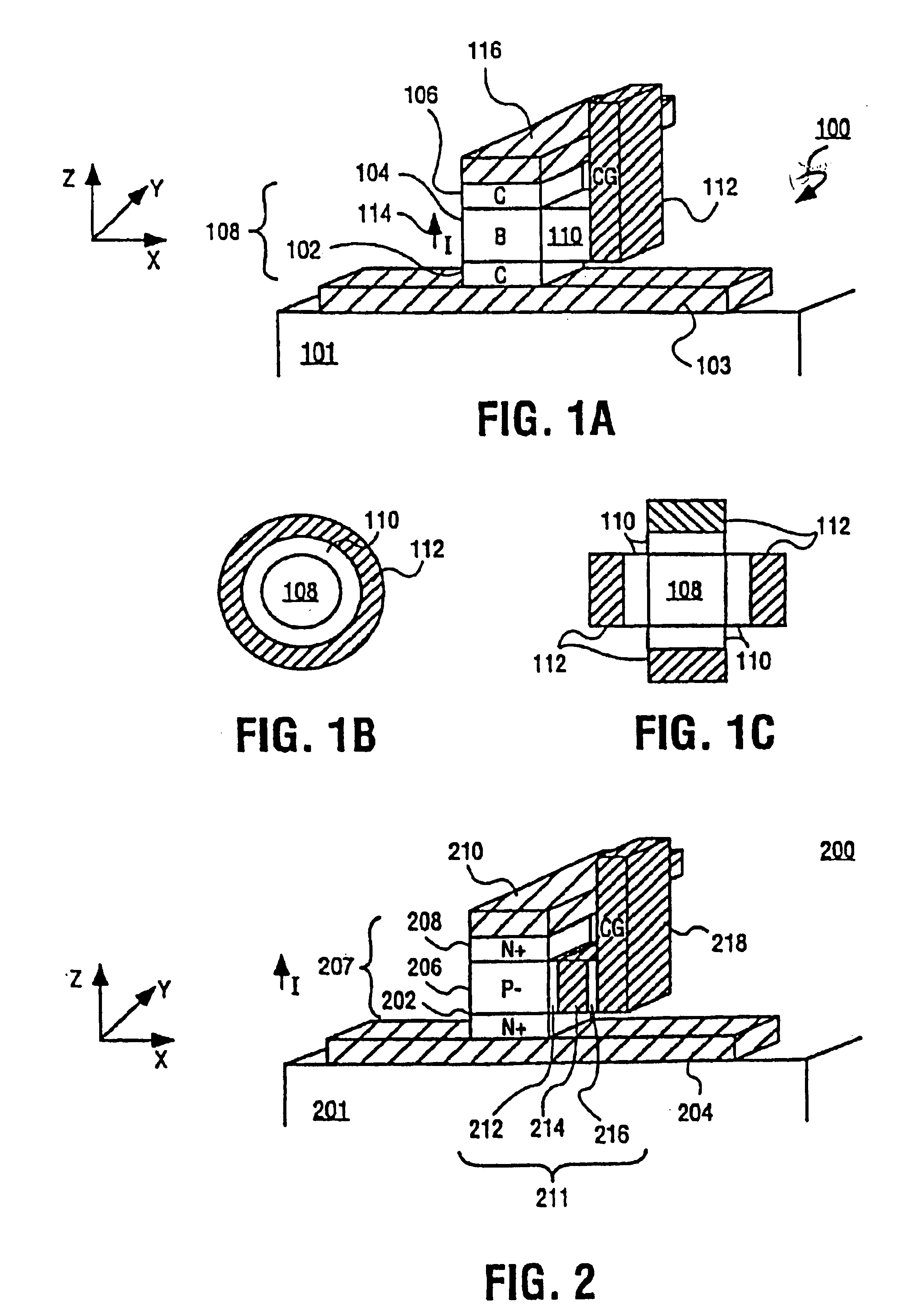
[0124]An embodiment of the present invention is a three terminal nonvolatile stackable pillar memory device. A pillar memory device 100 in accordance with this embodiment of the present invention is broadly illustrated in FIG. 1A. Pillar memory device 100 includes a first contact region 102 formed on a first input / output (I / O) 103 conductor formed on or above a plane (x-y) of a single crystal substrate 101. A semiconductor body 104 is formed directly on the first contact region 102 and a second contact region 106 is formed directly on the body 104. A second I / O conductor 116 is f...

first embodiment

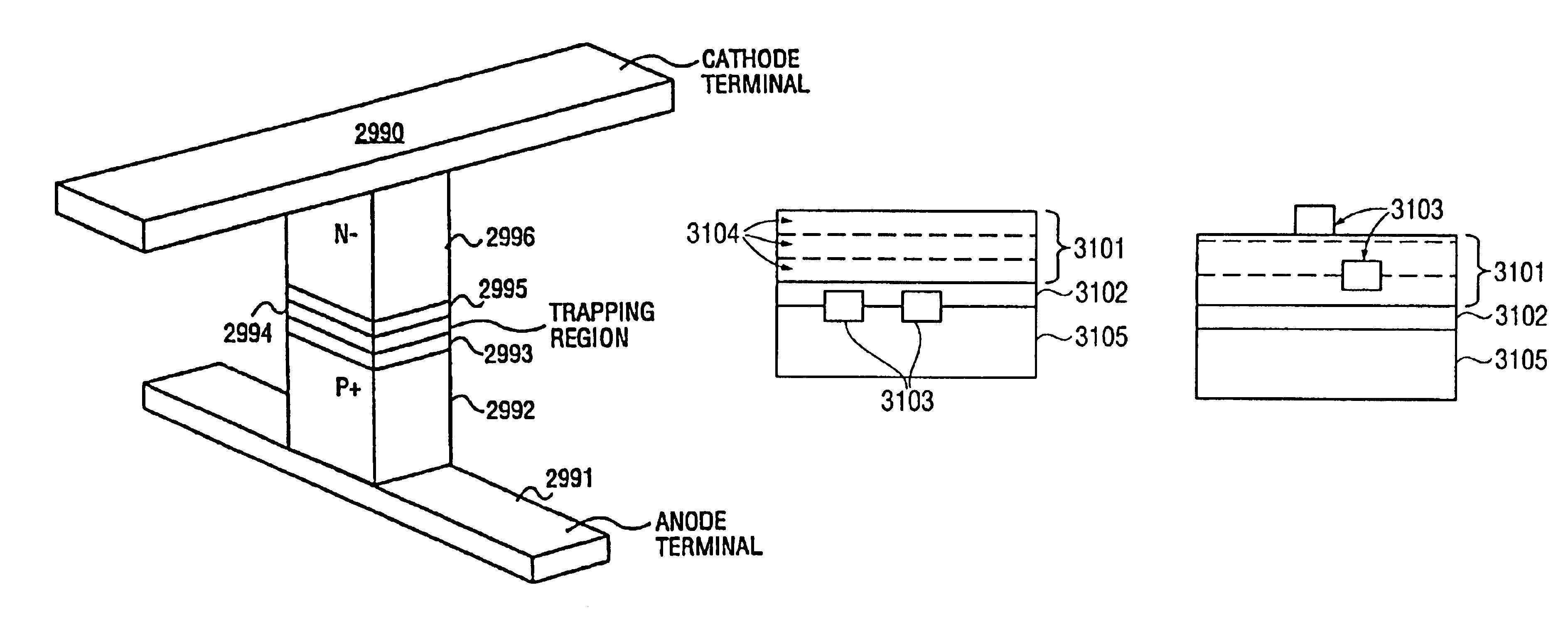
[0180]Referring to FIG. 30, the invented memory cell is illustrated disposed in a p-type substrate 2930. A diode (steering element of the cell) is formed in the substrate comprising an n− region 2932, doped, for instance to a level of 5×10¹⁶-1018 cm−3, and a p+ region 2931, doped to >1019 cm−3 formed within the n− region 2932. These regions may be formed with well-known methods such as diffusion or ion implantation.

[0181]A storage stack comprising a dielectric (e.g., oxide) region 2933, trapping layer 2934 and a second dielectric (e.g., oxide) region 2935 is formed on the region 2932.

[0182]The dielectric region 2933 may be a grown oxide layer or a deposited silicon dioxide region. When comprising oxide, this region may be 1-5 nm thick. Ordinary processing may be used to form these regions.

[0183]The trapping region 2934 and the other trapping regions discussed in this application may be formed from a compound of nitrogen as well as other materials. In the prior art, silicon nitride (...

fourth embodiment

[0255]In a preferred aspect of the fourth embodiment, the top surface of the upper portion of the floating gate 4310 is textured or roughened to further increase the capacitive coupling between the floating gate and the control gate / word line. For example, at least the upper portion of the floating gate 4310 may be made of hemispherical grain silicon (HSG), or the upper surface of the floating gate may be roughened by etching or coarse polishing. In other words, the upper portion of the floating gate may be textured or roughened similar to the texturing or roughening methods used to texture or roughen bottom conductive plates of DRAM capacitors.

[0256]While the first through fourth preferred embodiments describe and illustrate a TFT EEPROM nonvolatile flash memory array, the present invention should not be considered to be so limited. For example, rather than a self aligned word line in a TFT EEPROM array, any gate line may be self aligned to a MOSFET (i.e., metal oxide semiconductor...


PUM


Abstract

There is provided a monolithic three dimensional array of charge storage devices which includes a plurality of device levels, wherein at least one surface between two successive device levels is planarized by chemical mechanical polishing.

Description

[0001]This application is a continuation-in-part of U.S. application Ser. No. 09 / 801,233, filed on Mar. 6, 2001, now abandoned, which is a continuation-in-part of U.S. application Ser. No. 09 / 745,125, filed on Dec. 21, 2000, now abandoned, both of which are incorporated by reference in their entirety. This application is also a continuation-in-part of U.S. application Ser. No. 09 / 639,579 filed on Aug. 14, 2000, now abandoned, which is incorporated by reference in its entirety. This application is also a continuation-in-part of U.S. application Ser. No. 09 / 639,702 filed on Aug. 14, 2000, now abandoned, which is incorporated by reference in its entirety. This application is also a continuation-in-part of U.S. application Ser. No. 09 / 639,749 filed on Aug. 17, 2000, now abandoned, which is incorporated by reference in its entirety. This application also claims benefit of priority of provisional application Ser. No. 60 / 279,855 filed on Mar. 28, 2001, which is incorporated by reference in...

Claims


Application Information

Patent Timeline
Patent Type & Authority Patents(United States)
IPC IPC(8): H01L29/66H01L29/423H01L29/40H01L29/788H01L29/792H01L27/06H01L29/861H01L21/20H01L21/336H01L21/822H01L21/8246H01L21/8247H01L27/10H01L27/112H01L27/12H01L29/786
CPCG11C16/3427H01L27/0688H01L27/112H01L27/115H01L27/11521H01L27/11551H01L27/11556H01L27/11568H01L27/11578H01L27/11582H01L27/1203H01L29/42324H01L29/42332H01L29/66825H01L29/66833H01L29/7881H01L29/792H01L29/7926H01L29/8616H01L27/11558H01L29/7889H01L27/11526H01L29/16H01L27/11573H01L29/1604H01L21/8221G11C2211/5612H01L27/12H01L27/1158G11C16/0466H10B20/00H10B41/20H10B43/20H10B41/27H10B43/30H10B69/00H10B41/30H10B43/27H01L29/42364H01L29/861G11C16/10G11C16/14G11C16/26H01L21/31053H01L21/76819H10B20/60H10B41/40H10B41/60H10B43/10H10B43/40H10B43/23H01L29/0626H01L29/511H01L29/517H01L29/518H01L23/528H01L23/5329H01L29/0661H01L29/513H01L29/7391H01L29/78642
Inventor LEE, THOMAS H.SUBRAMANIAN, VIVEKCLEEVES, JAMES M.WALKER, ANDREW J.PETTI, CHRISTOPHER J.KOUZNETZOV, IGOR G.JOHNSON, MARK G.FARMWALD, PAUL MICHAELHERNER, BRAD
Owner WODEN TECH INC
Why Eureka
Try Eureka