Junction varactor with high Q factor and wide tuning range

a varactor and high q factor technology, applied in the field of mos varactors, can solve the problems of low maximum to minimum capacitance ratio, small quality factor, abrupt transition of maximum to minimum capacitance of mos varactors, etc., and achieve the effect of improving the electrical performance of mos varactors

Active Publication Date: 2005-04-19
UNITED MICROELECTRONICS CORP
View PDF13 Cites 15 Cited by
  • Summary
  • Abstract
  • Description
  • Claims
  • Application Information

AI Technical Summary

Benefits of technology

[0009]It is therefore a primary object of the claimed invention to provide a varactor to improve the electrical performance thereof.

Problems solved by technology

The main drawback of the prior art PN junction varactor as set forth in FIG. 1 is a low maximum to minimum capacitance ratio and small quality factor (Q factor).
However, the MOS varactor's transition from maximum to minimum capacitance is abrupt.

Method used


Image

  • Junction varactor with high Q factor and wide tuning range
  • Junction varactor with high Q factor and wide tuning range
  • Junction varactor with high Q factor and wide tuning range

Examples


Embodiment Construction

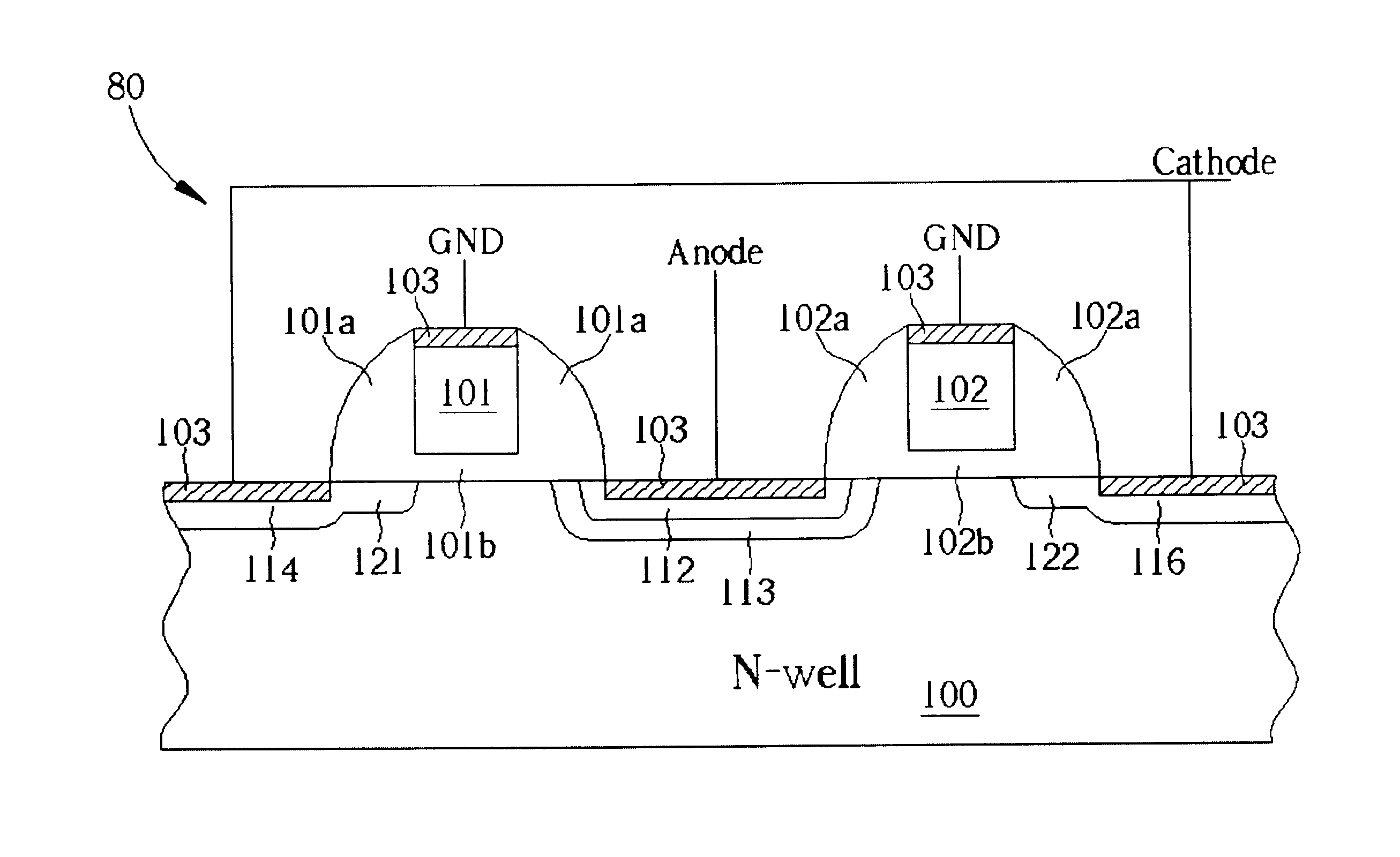
[0019]The present invention, which provides novel junction varactors for CMOS and BiCMOS technologies as well as a method for fabricating the same, will now be described in more detail by referring to the drawings that accompany the present application. It is to be understood that the conductivity types, device or circuit layout, or materials used as set forth in the following detailed description and figures are only for illustration purpose. The scope of this invention should be construed as limited only by the metes and bounds of the appended claims.

[0020]Referring initially to FIG. 3 and FIG. 4, wherein FIG. 3 is a schematic top view showing the basic layout of a junction varactor 80 in accordance with one preferred embodiment of the present invention, FIG. 4 is a schematic cross-sectional diagram showing the junction varactor 80 along line AA of FIG. 3. According to the preferred embodiment of the present invention, the junction varactor 80 is formed on an N-well 100, which may...


PUM


Abstract

A PN-junction varactor includes a first ion well of first conductivity type formed on a semiconductor substrate of second conductivity type. A first dummy gate is formed over the first ion well. A first gate dielectric layer is formed between the first dummy gate and the first ion well. A second dummy gate is formed over the first ion well at one side of the first dummy gate. A second gate dielectric layer is formed between the second dummy gate and the first ion well. A first heavily doped region of the second conductivity type is located in the first ion well between the first dummy gate and the second dummy gate. The first heavily doped region of the second conductivity type serving as an anode of the PN-junction varactor. Second heavily doped regions of the first conductivity type located in the first ion well at one side of the first dummy gate that is opposite to the first heavily doped region and at one side of the second dummy gate that is opposite to the first heavily doped region, the second heavily doped regions being electrically connected to each other and serving as a cathode of the PN junction varactor.

Description

BACKGROUND OF INVENTION[0001]1. Field of the Invention[0002]he present invention relates generally to a varactor, and more particularly, to a PN-junction varactor having improved quality factor (Q factor) and extended tuning range.[0003]2. Description of the Prior Art[0004]A varactor is, essentially, a variable voltage capacitor. The capacitance of a varactor, when within its operating parameters, decreases as a voltage applied to the device increases. Such a device is useful in the design and construction of oscillator circuits now commonly used for, among other things, communications devices. Varactors are typically employed in voltage-controlled oscillators (VCOs) where a frequency of an oscillator is controlled by an applied current or voltage. In such instances, the VCOs are used when a variable frequency is required, or when a signal needs to be synchronized to a reference signal.[0005]Numerous varactors have been developed and are employed in integrated circuit technologies, ...

Claims


Application Information

Patent Timeline
Patent Type & Authority Patents(United States)
IPC IPC(8): H01L29/66H01L27/08H01L29/93
CPCH01L27/0808H01L29/93H01L27/0811
Inventor GAU, JING-HORNGCHEN, ANCHOR
Owner UNITED MICROELECTRONICS CORP
Why Eureka
Try Eureka