Integrated color LED chip

a color led chip and integrated technology, applied in the direction of discharge tube luminescnet screens, discharge tube/lamp details, incadescent envelopes/vessels, etc., can solve the problems that the complexity and cost of devices have prohibited the use of the majority of such systems, and achieve the reduction of cross-talk, the effect of improving contrast and minimizing the cross-talk due to substrate reflections

Inactive Publication Date: 2005-04-19
KYMA TECH
View PDF5 Cites 90 Cited by
  • Summary
  • Abstract
  • Description
  • Claims
  • Application Information

AI Technical Summary

Benefits of technology

[0007]In at least one embodiment of the invention, opaque material is deposited between adjacent light emitting regions thereby minimizing cross-talk and achieving improved contrast. In at least one other embodiment of the invention, cross-talk due to substrate reflections is minimized by removing the light emitting...

Problems solved by technology

Although LCD display based systems have proven adequate for some applications, ...

Method used


Image

  • Integrated color LED chip
  • Integrated color LED chip
  • Integrated color LED chip

Examples


Embodiment Construction

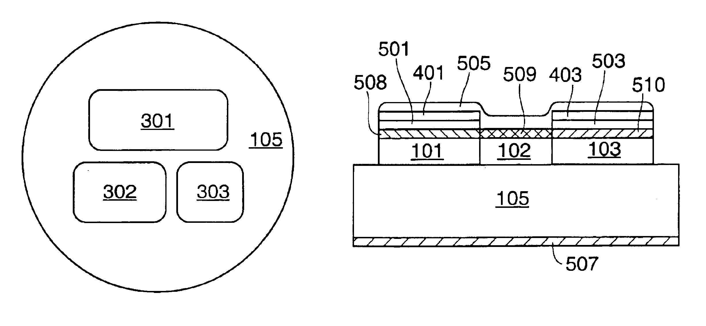
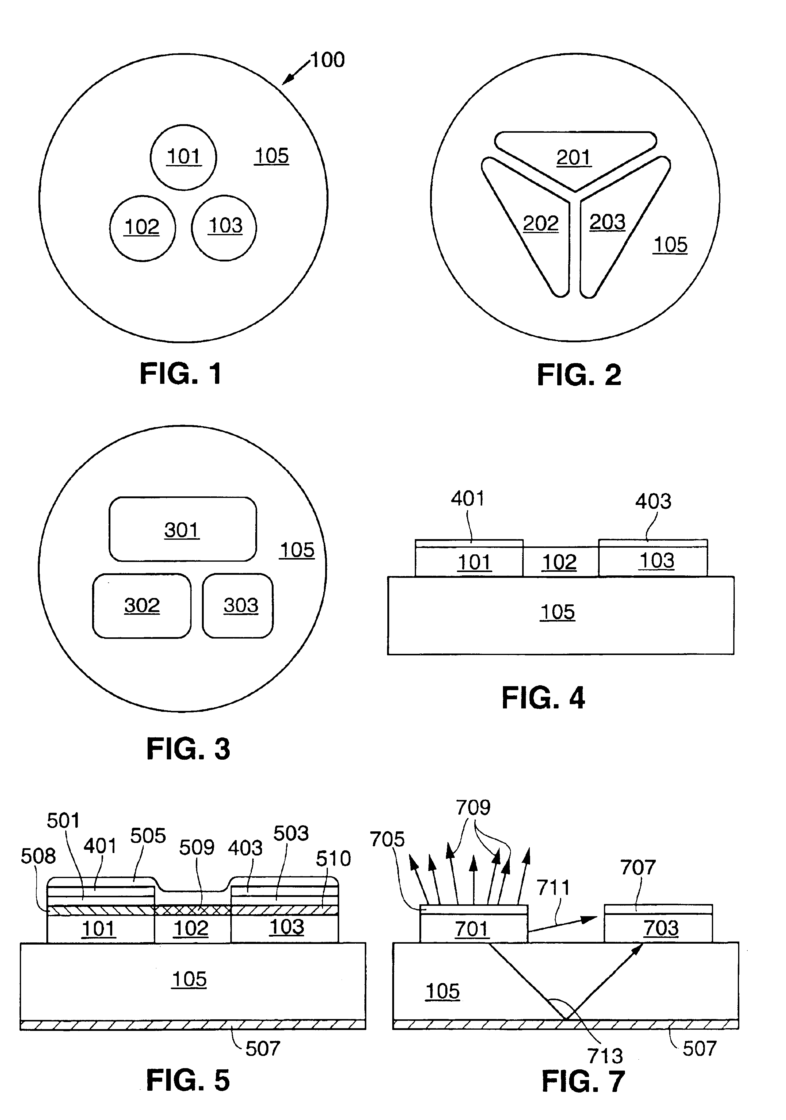
[0024]FIG. 1 is an illustration of an embodiment of the invention. In the embodiment shown, an integrated color chip (ICC) 100 contains a single set of color emitting regions 101-103 residing on a single substrate 105 (e.g., a substrate comprised of sapphire, silicon carbide, gallium nitride, etc.). Preferably light emitting regions 101-103 are in sufficiently close proximity to one another to facilitate color integration by an observer. It will be understood that as the apparent distance between ICC 100 and the observer increase, the required spacing between light emitting regions 101-103 increases. Although each light emitting region 101-103 is illustrated as having a circular shape, it is understood that the inventor envisions other shapes. For example, as shown in FIG. 2, light emitting regions 201-203 are non-circular in order to achieve improved packing density. Alternately, as shown in FIG. 3, light emitting regions 301-303 are of different dimensions, the dimensional variati...


PUM


Abstract

A method and apparatus for achieving multicolor displays using an integrated color chip is provided. The integrated color chip contains one or more multicolor generation sites on a single substrate. Each multicolor generation site is comprised of two or more light emitting regions in close proximity to one another, the number of light emitting regions per site dependent upon the number of required colors. The active light generation system for each light emitting region, e.g., an LED, is preferably identical in device structure although size and shape may vary. In order to achieve the desired colors, one or more light conversion layers are applied to individual light emitting regions. Each light emitting region may also include index matching layers, preferably interposed between the outermost surface of the light emitter and the light conversion layer, and protective layers. In order to minimize cross-talk and achieve improved contrast, opaque material is preferably deposited between adjacent light emitting regions. Cross-talk may also be minimized by locating the light emitting regions on a substantially non-reflective substrate.

Description

CROSS-REFERENCES TO RELATED APPLICATIONS[0001]This application is a continuation of U.S. patent application Ser. No. 09 / 891,972, filed Jun. 26, 2001, now U.S. Pat. No. 6,737,801, which claims benefit from Provisional Application Ser. No. 60 / 214,505, filed Jun. 28, 2000.FIELD OF THE INVENTION[0002]The present invention relates generally to multicolor display devices and, more particularly, to a method and apparatus for achieving multiple colors on an integrated chip.BACKGROUND OF THE INVENTION[0003]Multicolor generation systems are used in a variety of applications including monitors (e.g., direct and projection televisions, computer monitors), macro-displays (e.g., billboards), and micro-displays (e.g., telephones and PDAs). Currently a number of different techniques are used to achieve multicolor displays. For example, depending upon application requirements such as contrast, brightness, color range, color accuracy, power consumption, size and cost, a display may utilize light gene...

Claims


Application Information

Patent Timeline
IPC IPC(8): H01L27/15H01L33/00H01L33/50
CPCH01L27/156H01L33/504
Inventor RAGLE, LARRY
Owner KYMA TECH
Why Eureka
Try Eureka